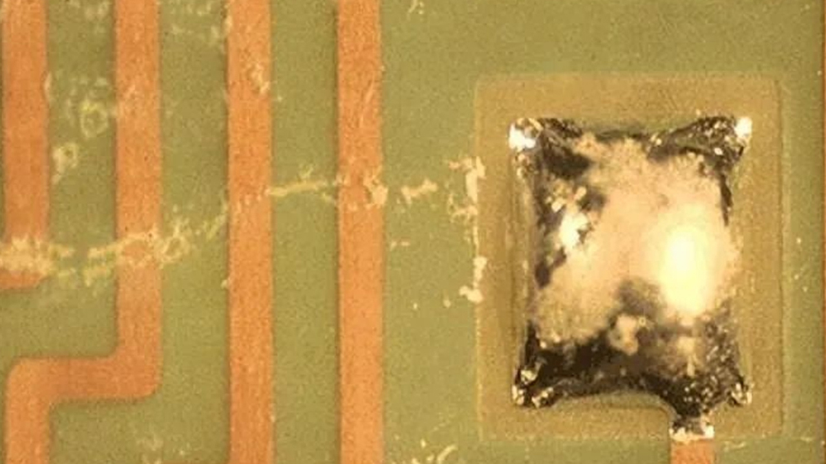
Semiconductor Packaging Inspection & Rework

Semiconductor packages and electronic modules contain solder balls, thermal pads, lead frames and internal connections that cannot always be examined from the outside.
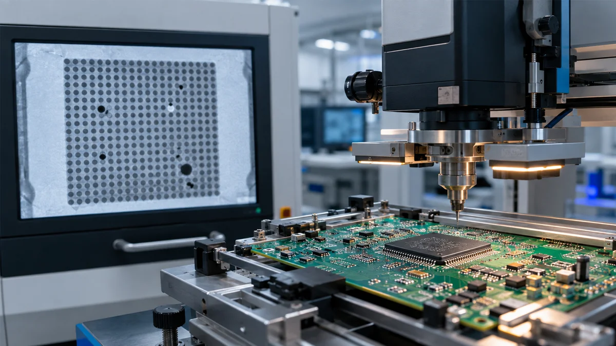
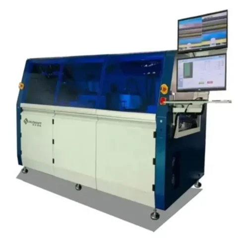
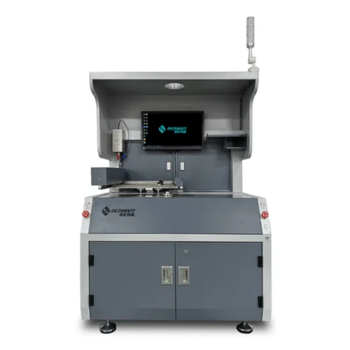
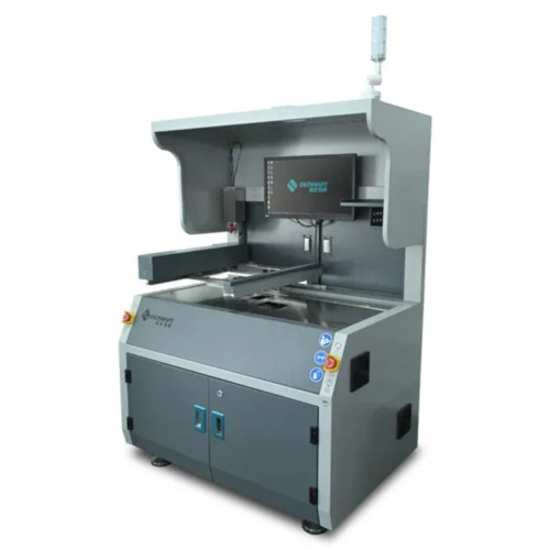
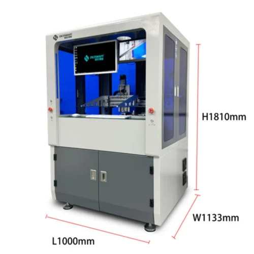
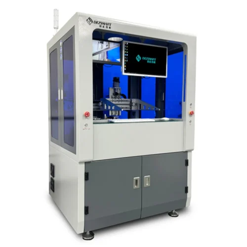
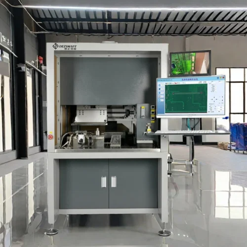
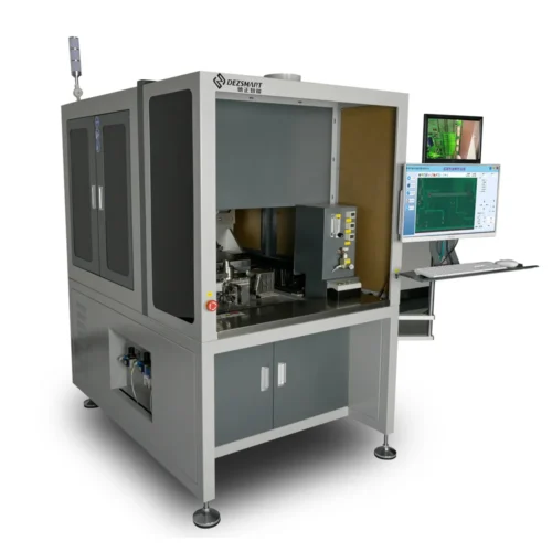
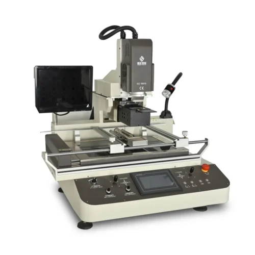
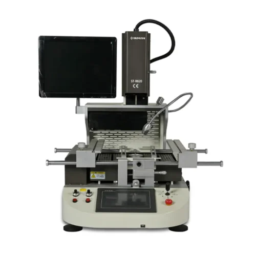
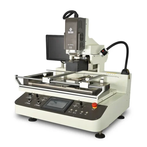
DEZ X-ray systems inspect internal package structures and board-level solder connections without cutting the sample. X-ray component counters measure parts inside tape-and-reel packaging, while BGA rework stations remove and replace failed packages on assembled PCBs and modules.

What DEZ Equipment Covers

Semiconductor Package Inspection

Examine internal structural conditions and connection states inside compatible IC packages, power devices and electronic modules.

BGA and Bottom-Terminated Package Inspection

Inspect solder balls and solder distribution beneath BGA, QFN, LGA, CSP and other packages after board or module assembly.
Thermal-Pad Void Inspection

Measure void areas and compare solder distribution beneath compatible power packages and exposed thermal pads.
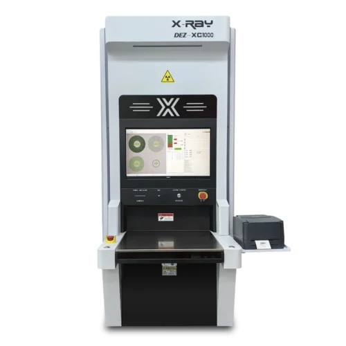
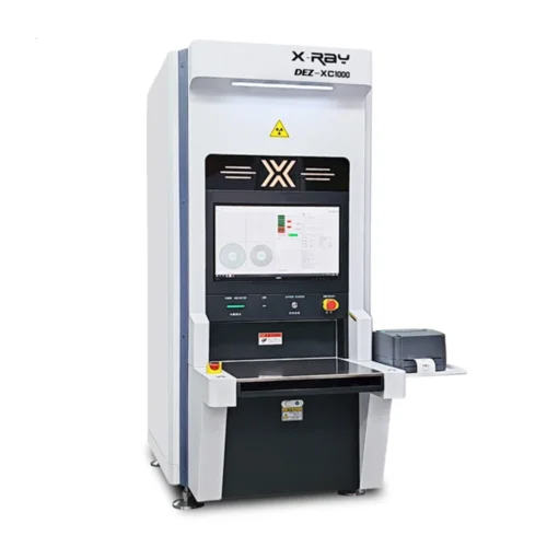
Tape-and-Reel Component Counting

Count electronic components inside sealed reels without unwinding the carrier tape.

Package Replacement on PCB Assemblies

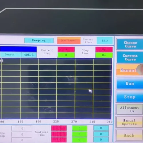
Remove, align and replace BGA, QFN, CSP, QFP, POP and other compatible surface-mounted components.

Post-Rework Inspection

Inspect replaced components again to check solder-ball position, bridging, voiding and solder distribution.

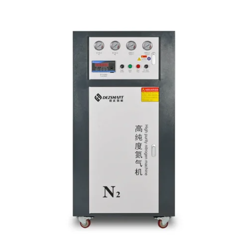
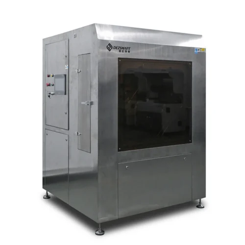
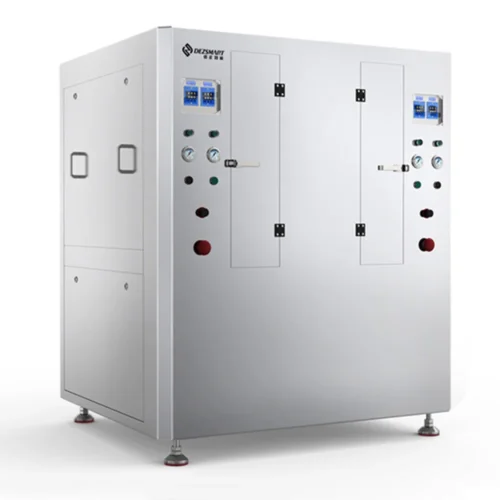
Recommended Inspection and Rework Equipment

Semiconductor Inspection FAQ

Which Machine Inspects Semiconductor Packages?

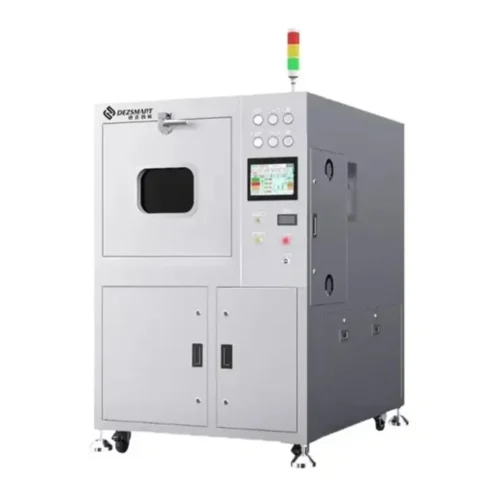
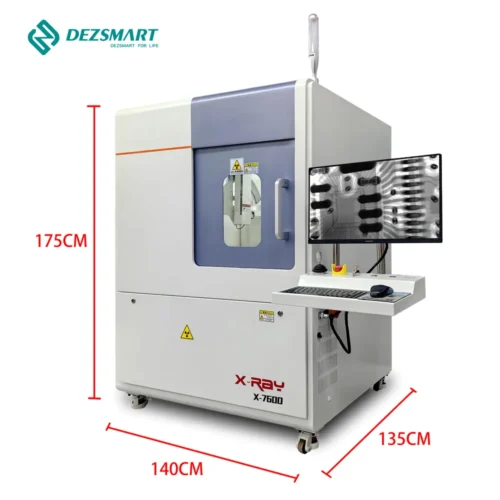
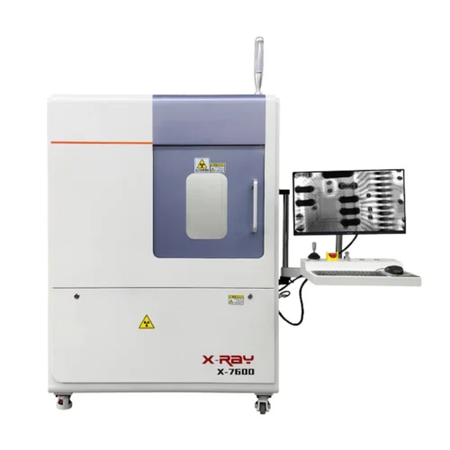
Choose the DEZ-X7600 for compatible packages, modules and board-level solder joints. Final image quality depends on the package size, density, material overlap and defect location.

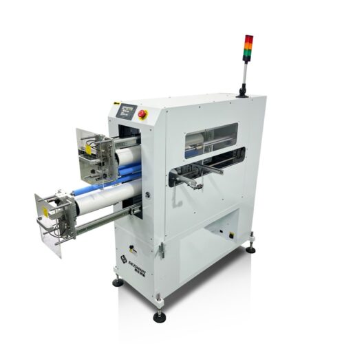
Choose the DEZ-XC1000. It supports 7–17-inch reels and components as small as 01005.

The DEZ-X7600 provides void-area calculation for compatible solder joints and thermal pads.

Choose the DEZ-R820 for components from 2 × 2 mm to 80 × 80 mm and PCBs up to 415 × 370 mm.

Choose the DEZ-R880A for components up to 120 × 120 mm and assemblies up to 710 × 490 mm.

Provide the package or module dimensions, materials, expected internal structure, suspected defect, required inspection detail and any existing X-ray or electrical-test results.

Request a Semiconductor Inspection Solution

Send us the package, module or PCBA dimensions, sample weight, internal structure, suspected defect and required image detail.

For component counting, provide the reel diameter, component dimensions, carrier-tape structure and expected quantity range.

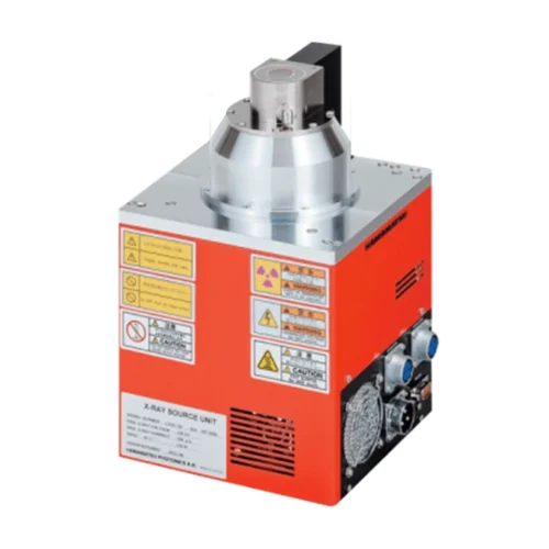
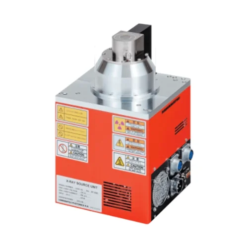
DEZ will recommend the DEZ-X7600, DEZ-XC1000, a BGA rework station or a microfocus X-ray source according to the actual task.

Drag & Drop Files, Choose Files to Upload, or Capture With Your Camera

Related SMT Process Articles

We share our SMT manufacturing expertise to help you optimize soldering, PCBA cleaning, inspection, and production efficiency.