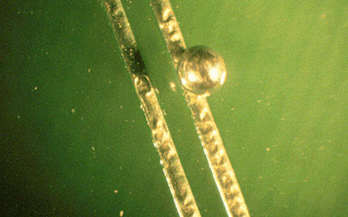
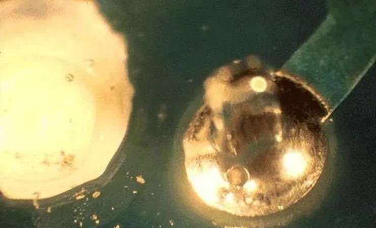
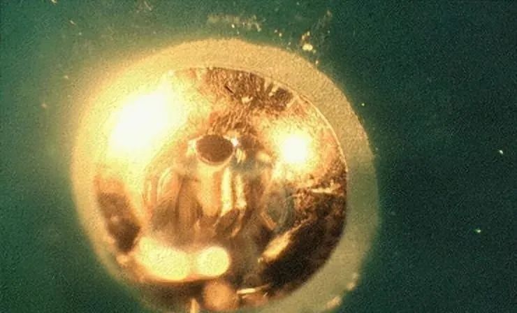
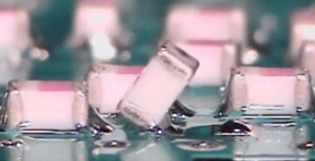
Most wave soldering defects come from five areas: solderability, flux application, preheating, solder-wave control or PCBA design.
Do not correct every defect by increasing solder temperature or contact time. First determine whether the problem affects one joint, one component, one board position or the complete production batch. The defect pattern usually indicates where to begin.
Table of Contents
How Does Wave Soldering Work?
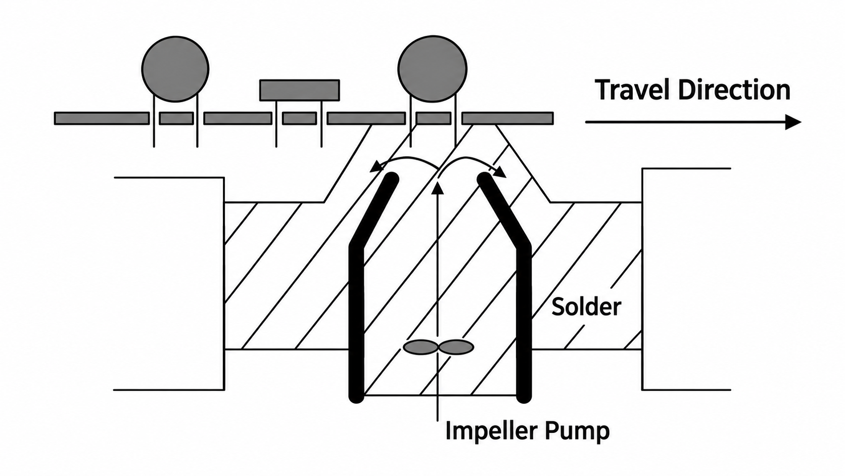
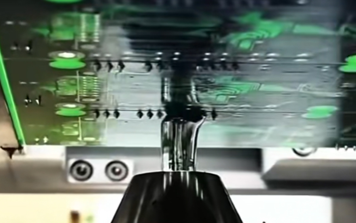
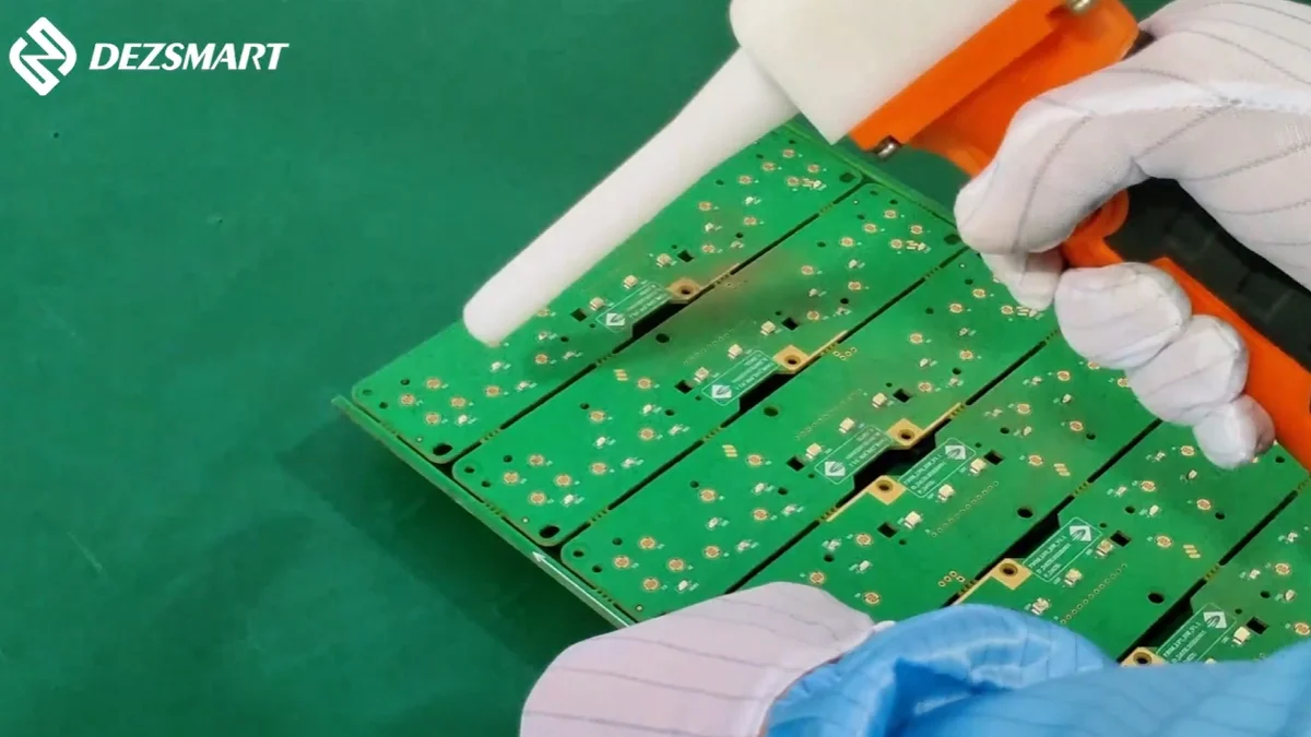
Wave soldering is mainly used to solder THT components to a PCB. Flux is applied to the solder side, the assembly is preheated, and the underside passes over a controlled wave of molten solder.
The flux removes light oxides and supports wetting. Preheating activates the flux, removes part of its solvent and reduces the temperature difference when the PCBA reaches the solder wave.
The solder then wets the component leads, pads and plated through-holes. As the board leaves the wave, excess solder drains away and the remaining solder forms the joints.
Common Wave Soldering Defects: Quick Diagnosis
Defect
Visible evidence
Check first
Solder bridging
Solder joins adjacent pins or pads
Component orientation, lead length, conveyor speed, wave height and exit conditions
Insufficient hole fill
Solder does not rise far enough through the plated hole
Flux penetration, preheat, contact time, thermal mass and hole-to-lead fit
Non-wetting or cold joint
Solder does not bond correctly to the pad or lead
Oxidation, contamination, flux activity and solderability
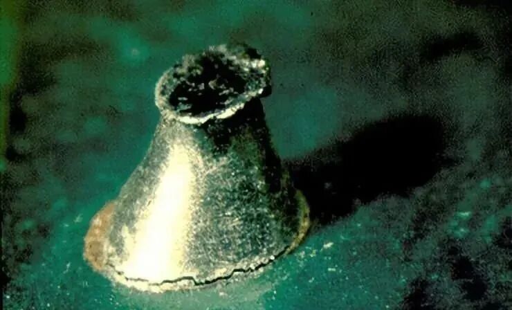
Excess solder or icicles
Heavy fillet or pointed solder projection
Wave stability, conveyor angle, lead length, solder temperature and withdrawal
Solder balls or spatter
Loose or attached solder spheres around the joint
Moisture, wet flux, preheating, solder-mask condition and wave turbulence
Pinholes or blowholes
Small holes in or through the solder joint
PCB moisture, outgassing, contamination and through-hole plating
Lifted component
THT component rises from the PCB
Insertion depth, lead length, board warp, fixture support and wave force
Lifted pad or damaged solder mask
Copper pad or coating separates from the board
Excess heat, mechanical force, PCB material and fabrication quality
Cracked solder joint
Crack appears around the lead, pad or fillet
Board flex, component movement, thermal stress and joint design
Flux residue
White, brown, clear or sticky material remains
Flux quantity, preheat profile, flux compatibility and cleaning process
A visual symptom is not a complete diagnosis. Measure the process before changing it.
Why Do Solder Bridges Form?
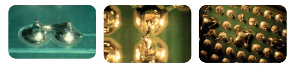
A solder bridge forms when solder remains between adjacent pins or pads after the PCBA leaves the wave.
Common causes include close pin spacing, long leads, poor board orientation, an unstable or excessive wave, incorrect conveyor speed and weak solder peel-off. PCB design and the direction in which a long connector enters the wave can also change the bridging rate. IPC testing has shown that component orientation, conveyor speed, solder-pot temperature and wave configuration can affect THT bridging.
Check whether bridging occurs on the same end of each connector. If it does, review board orientation and solder drainage first. If bridges appear across the complete board, inspect the wave, conveyor and solder condition.
Reducing solder temperature without checking hole fill can create a second problem. Change one parameter at a time and inspect both bridging and barrel fill after each trial.
Why Is the Plated Through-Hole Not Filled?
Insufficient hole fill means solder has not reached the required level inside a plated through-hole.
When many joints on the board show the same problem, check flux coverage, preheat and wave contact. Too little flux, weak flux activation, excessive drying before wave contact, low preheat or insufficient solder-contact time can all reduce fill.
When one connector or one ground pin is affected, compare its thermal load with nearby joints. Thick boards, internal copper planes, large terminals and tight hole-to-lead relationships can remove heat from the joint.
A useful sequence is to verify flux penetration, measure the topside temperature, confirm solder-wave contact and then check the PCB finish, hole plating and component-lead solderability. Do not copy a fixed preheat temperature from another PCBA.
Is a Dull Joint Always a Cold Solder Joint?
No. Some lead-free solder joints have a naturally duller surface than traditional tin-lead joints.
A cold or poorly wetted joint should be identified from the complete joint shape and wetting condition, not from shine alone. Warning signs include exposed pad areas, poor contact angles, irregular fillets and solder that has not bonded to the pad or lead.
The main checks are solderability, surface oxidation, contamination, flux activity, preheat and solder contact. Reheating may repair an individual joint, but repeated cold joints require correction of the production process.
What Causes Excess Solder, Icicles and Webbing?
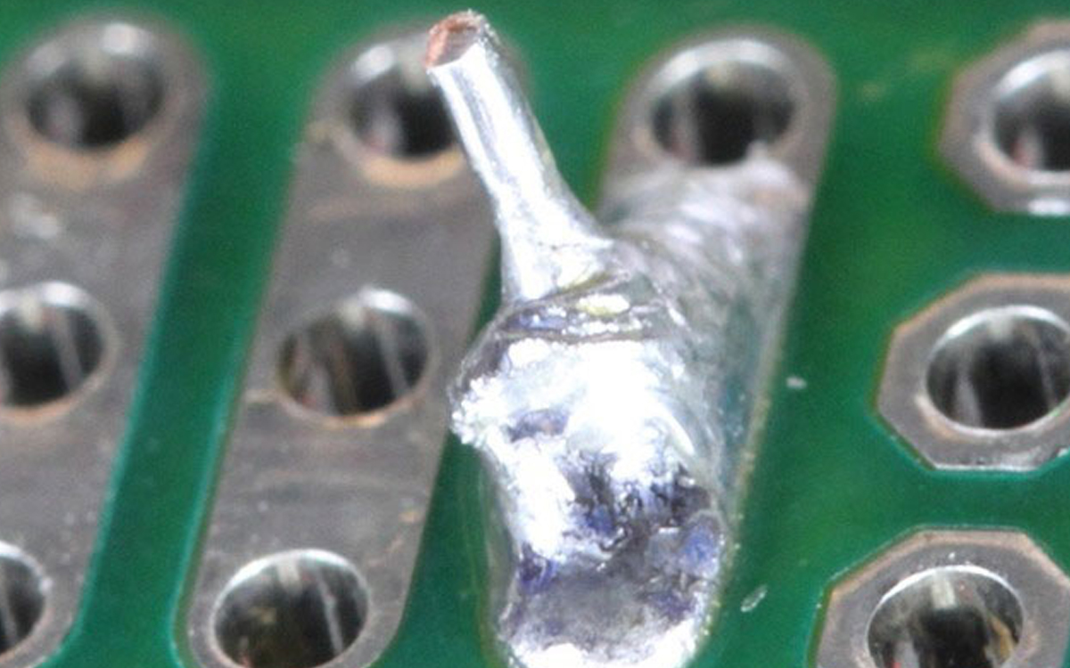
Excess solder may appear as a heavy fillet, a long point or thin solder webbing between features.
The solder may not separate cleanly from the PCBA because of incorrect conveyor angle, long component leads, unstable wave height, unsuitable solder temperature, poor flux activity or contaminated solder. Indium identifies wave height, preheat, conveyor speed, solderability and flux condition among the causes of wave-solder icicles.
Inspect where the excess solder forms. A repeated icicle at the same lead suggests a local geometry or drainage problem. Random webbing across the solder side points more strongly to wave stability, flux or solder condition.
What Causes Solder Balls and Spatter?
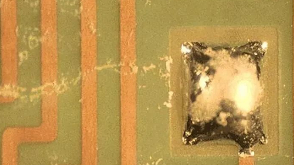
Solder balls can form when moisture or flux solvent releases gas as the PCBA contacts the solder wave. Wave turbulence, excess flux, unsuitable preheating and some solder-mask surfaces can also contribute.
Preheating must remove enough solvent without exhausting the flux activity before soldering. It also warms the PCB and components so that soldering can occur within a controlled contact time.
Remove loose solder balls before the assembly moves to electrical testing or final assembly. However, cleaning only removes the result. It does not correct excess flux, moisture or unstable wave conditions.
What Causes Pinholes and Blowholes?
Pinholes and blowholes form when gas escapes through molten solder before the joint has fully solidified.
Possible sources include moisture in the PCB, volatile material, contamination and outgassing from the plated through-hole. Poor hole plating or damaged hole walls can also contribute.
Check whether the defect follows the same PCB lot, hole type or component. If it does, inspect board storage, baking history, fabrication quality and hole plating before changing the complete wave process.
Why Do Components, Pads or Solder Mask Lift?
A THT component may rise when it was not fully inserted, its leads are too long, the board bends or the solder wave applies excessive force. The fixture must hold the assembly without blocking required solder access.
This should not automatically be called tombstoning. Tombstoning normally describes an SMT component standing on one end during reflow because of unbalanced wetting forces.
A lifted pad is a different failure. It can result from excessive heat, repeated rework, mechanical force, weak copper adhesion or handling the assembly while it is still hot.
Solder-mask blistering or peeling can indicate poor PCB preparation, trapped moisture, weak curing or thermal incompatibility. Changing the soldering profile cannot correct a defective PCB coating.
Why Do Solder Joints Crack?
Cracks can result from board flex, repeated movement, component stress, thermal expansion or weak adhesion between the solder and pad.
Do not treat every crack by simply reheating the joint. First identify whether the crack is inside the solder, at the pad interface or connected to a lifted pad.
If several assemblies fail in the same position, inspect the PCB support, component mass, lead forming and handling method. A design or mechanical-load problem will return after local repair.
What Does Flux Residue After Wave Soldering Mean?
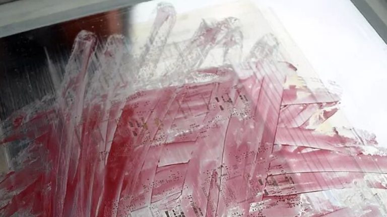
Visible flux residue may appear white, brown, clear or sticky. Its appearance depends on the flux chemistry, applied quantity, preheating, solder exposure and any cleaning process.
No-clean flux does not mean residue is never a concern. The residue must remain acceptable for the actual product, operating environment, coating process and customer requirement.
Visible residue does not prove the level of ionic contamination. Flux residue can be a source of ionic contamination, but cleanliness must be checked with the specified test method when an ionic limit applies.
Also use the correct term: flux residue remains after soldering. Solder mask is the permanent protective coating on the PCB.
How Should Wave Soldering Defects Be Troubleshot?
Start by marking the exact defect location and checking whether it repeats on the same component, board position, machine lane or production lot.
Next, confirm the PCB finish, component-lead condition, flux type and solder alloy. Material changes can move the process outside its previous working window.
Measure flux deposition, board temperature, conveyor speed, contact time, wave height and solder temperature. Machine setpoints alone do not prove what the PCBA experienced.
Change one variable at a time. Then inspect the complete joint, not only the original symptom. A change that reduces bridging may also reduce hole fill.
Finally, validate the corrected process against the applicable drawing, customer requirement and assembly-acceptance criteria.
When Is Selective Soldering Better Than Full-Wave Soldering?
Full-wave soldering remains practical when most of the underside can contact the wave and many THT joints must be soldered together.
Consider selective soldering when a mixed SMT/THT assembly has only defined through-hole joints, while nearby SMD components or protected areas should not enter a full solder wave.
For offline production requiring lower infrared preheating, the DEZ-H3600A processes a maximum soldering area of 400 × 300 mm.
For automatic carrier transfer, use the DEZ-H3800S when sequential processing meets the required takt. Use the DEZ-H3900A for larger carriers or separate fluxing, preheating and soldering stations.
Selective soldering can reduce unnecessary full-wave exposure, but it does not correct poor solderability, inaccessible joints or an unsuitable PCB design.
Which DEZ Machine Removes Residue and Loose Solder Balls?
First correct the soldering process. Cleaning should not be used to hide recurring fluxing, moisture or wave-control problems.
For selective soldering or post-solder cleaning evaluation, send clear defect photos, the PCBA drawing, affected THT coordinates, board dimensions, production volume and required takt time.
Also provide the PCB thickness, solder alloy, flux type, current preheat and solder settings, cleanliness requirement and available factory utilities.
DEZ can then determine whether the problem requires process correction, selective soldering, solder-side brush cleaning or complete aqueous PCBA cleaning.