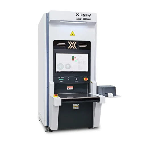
PCBA X-Ray Inspection System for BGA and Hidden Solder Joints | DEZ-X7600

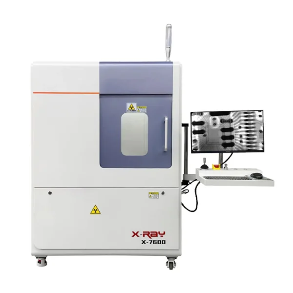
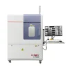
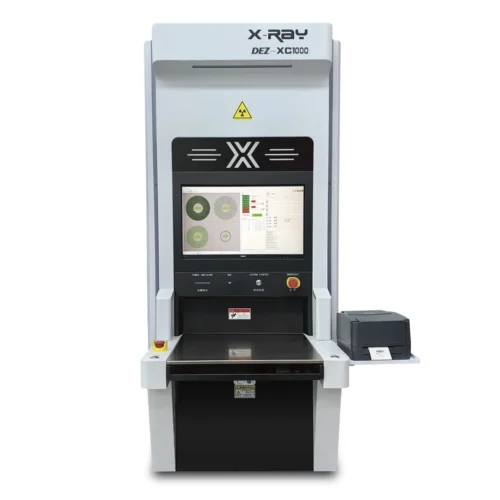
The DEZ-X7600 PCBA X-Ray Inspection System uses high-resolution X-ray imaging to examine solder joints and internal structures that are hidden beneath electronic components.

It allows quality engineers to inspect BGA, QFN, LGA, CSP, semiconductor and other bottom-terminated components without cutting, opening or damaging the PCB assembly.

The 130 kV closed microfocus X-ray source, 5 μm focal spot and up to 150× geometric magnification reveal internal solder distribution, component position and connection conditions in real time.

By finding hidden defects before products leave the factory, the DEZ-X7600 helps manufacturers reduce repeated failures, prevent defective assemblies from reaching the next process and identify the real cause of soldering problems.

Inspection Capability Problem It Helps Identify
Hidden solder-joint imaging Defects beneath BGA, QFN, LGA and CSP packages
High-resolution magnification Small solder balls, fine-pitch joints and internal structures
Oblique-angle inspection Overlapping joints that are difficult to separate in a vertical image
Real-time image display Rapid defect confirmation during inspection
Void-area calculation Excessive voiding within solder joints or thermal pads
Distance and size measurement Solder-ball diameter, spacing and defect dimensions
Large inspection platform PCBs and assemblies up to 510 × 450 mm
12 kg platform capacity Large or heavy electronic assemblies
Image and result storage Quality records, failure analysis and process comparison
Non-destructive inspection Preserves the assembly for rework or further testing
Drag & Drop Files, Choose Files to Upload, or Capture With Your Camera
SKU: PCBA-X-Ray-Inspection-System-X7600 Category:
Share your love

Find Defects Hidden Beneath Components

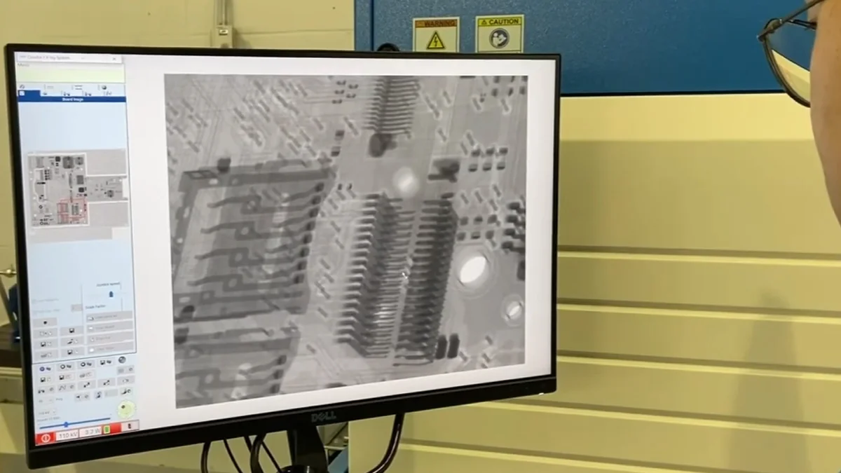
AOI and visual inspection can examine component position, polarity and visible solder fillets. They cannot directly see solder joints located underneath a BGA, QFN or other bottom-terminated package.

A board can therefore appear correct from the outside while containing defects such as: Solder bridging, Missing solder balls, Insufficient solder, Excessive solder, Solder voids, Component misalignment, Uneven solder-ball shape, Open-joint indications, Foreign material, Internal package damage.

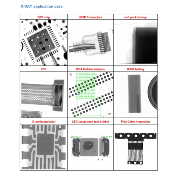
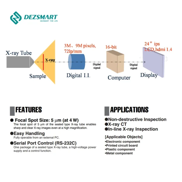
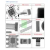
The DEZ-X7600 transmits X-rays through the assembly and converts differences in material density into a visible image. Solder absorbs more X-ray energy than the surrounding PCB and component materials, allowing hidden solder joints to appear clearly on the inspection screen.

This gives quality engineers direct visual evidence instead of relying only on electrical symptoms or external appearance.

PCBA-X-Ray-Inspection-System-Display-Details

Applications of the PCBA X-Ray Inspection

BGA and CSP Inspection

Inspect hidden solder-ball arrays for bridging, missing joints, irregular ball shape, voids and component displacement.

QFN and LGA Inspection

Evaluate central thermal-pad solder coverage, voiding and hidden peripheral connections.

SMT Process Verification

Inspect first-article PCBAs and compare soldering results after changes to stencil design, paste volume, placement or reflow settings.

PCBA Failure Analysis

Examine suspect components after functional or electrical test failures without immediately removing them from the PCB.

Rework Quality Verification

Inspect BGA or QFN joints after component removal, rebelling or replacement to confirm the quality of the rework result.

Semiconductor and Electronic Component Inspection

Observe internal package structures, bond regions, connectors and other density differences in compatible electronic components.

Incoming Component Verification

Inspect high-value or suspect components before they enter production when internal condition or package integrity must be evaluated.
PCBA-X-Ray-Inspection-System-Detecting

Inspect Without Damaging the PCBA

Traditional destructive analysis may require cutting the PCB, removing a component or preparing a cross-section.

These methods can provide detailed evidence, but the inspected board can no longer be returned directly to production.

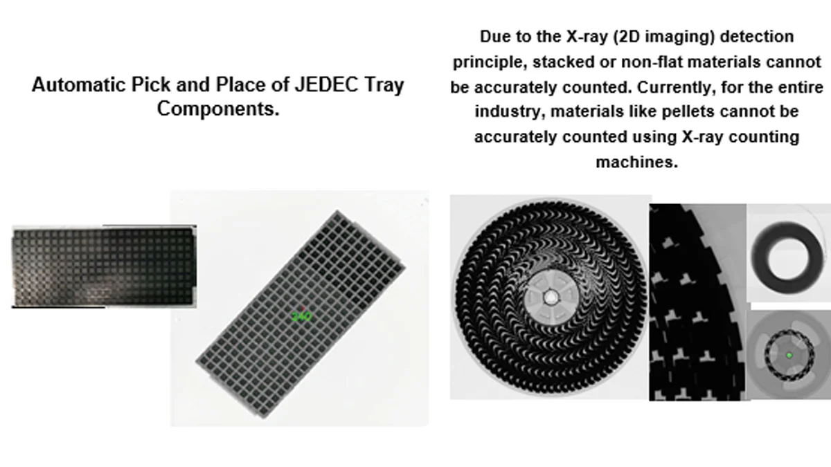
The X-ray component counter does not need to unwind the tape. Operators place the complete reel inside the machine and receive the count from a single scan.

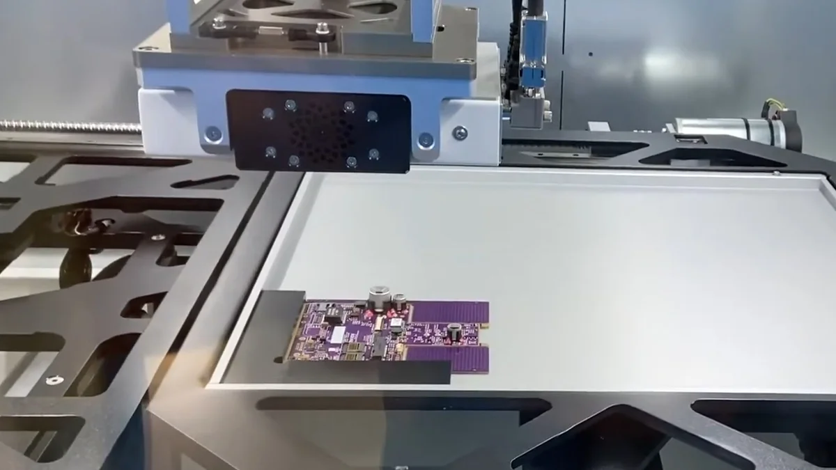
The DEZ-X7600 performs non-destructive inspection through the complete assembly. The PCBA remains intact and non-destructive X-ray inspection is particularly valuable for high-cost PCBAs, low-volume products, engineering samples and assemblies containing expensive semiconductors.

PCBA X-Ray Inspection Technical Specifications

ParameterSpecification
BrandHamamatsu, Japan
TypeClosed microfocus X-ray tube
Maximum voltage130 kV
Current10–300 μA
Focus size5 μm
Maximum power39 W
Geometric magnificationUp to 150×

Flat-Panel Detector

ParameterSpecification
BrandiRAY
Detector typeAmorphous-silicon flat-panel detector
Imaging area130 × 130 mm
Pixel matrix1536 × 1536
Pixel size85 μm
Resolution5.8 lp/mm
Frame rate20 fps
Viewing angleMulti-angle inspection supported

Inspection Platform

ParameterSpecification
Loading area520 × 520 mm
Maximum inspection area510 × 450 mm
Maximum sample weight12 kg
X-axis travel510 mm
Y-axis travel450 mm
Detector Z-axis travel300 mm
X-ray source Z-axis travel300 mm
Control methodJoystick, mouse and keyboard
NavigationHigh-definition camera

Machine Specifications

ParameterSpecification
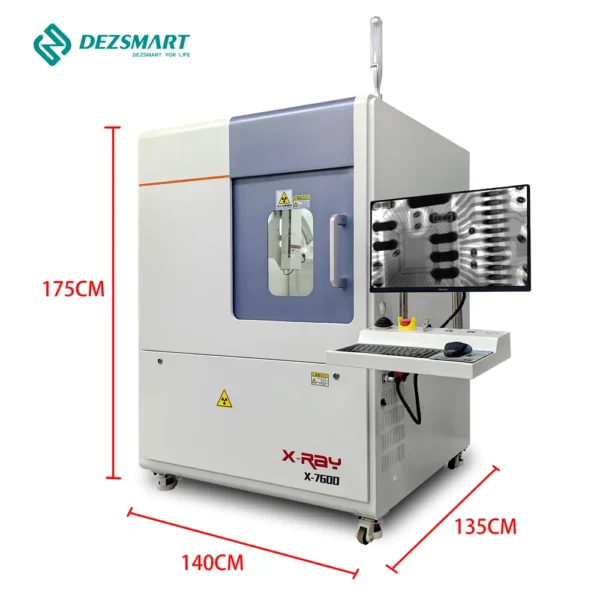
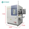
Machine dimensions1,400 × 1,350 × 1,750 mm
Machine weightApproximately 1,650 kg
Power supplyAC 220 V, 50 Hz
Maximum power2.0 kW
Industrial computerAdvantech industrial computer
ProcessorIntel i5-7700
Memory8 GB RAM
Storage1 TB HDD
Monitor24-inch FHD display
Listed radiation leakageBelow 0.5 μSv/h

X-Ray Inspection vs AOI

Inspection RequirementX-Ray InspectionAOI
Visible component positionYesYes
Visible solder filletsYesYes
Joints beneath BGAYesNo
QFN thermal-pad voidsYesNo
Internal solder distributionYesNo
Component labels and polarityLimitedYes
Surface contaminationLimitedYes
Internal package structureYesNo
Primary strengthHidden and internal defectsVisible surface defects

We are Proud to Partner with These Brands

We have worked with

DEZ-SMT-Partner-BAE-SYSTEMS DEZ-SMT-Partner-Dextra DEZ-SMT-Partner-eolane DEZ-SMT-Partner-Foxconn DEZ-SMT-Partner-IMI DEZ-SMT-Partner-JABIL DEZ-SMT-Partner-LACROIX DEZ-SMT-Partner-Laudren-Electronique DEZ-SMT-Partner-LEAB DEZ-SMT-Partner-MULTILASEr DEZ-SMT-Partner-RENISHAW DEZ-SMT-Partner-SANMINA DEZ-SMT-Partner-UNIVERSAL DEZ-SMT-Partner-Visteon

Continue the Inspection and Rework Process

Automatic-Pick-and-Place
After locating a hidden BGA defect, use controlled heating and positioning to remove or replace the affected component.
X-Ray Inspection & BGA Rework Solutions
Learn when X-ray inspection is required, which defects it can reveal and how it complements AOI and electrical testing.

Suitable Manufacturing Environments

Automotive-Electronics-SMT-1
Automotive Electronics
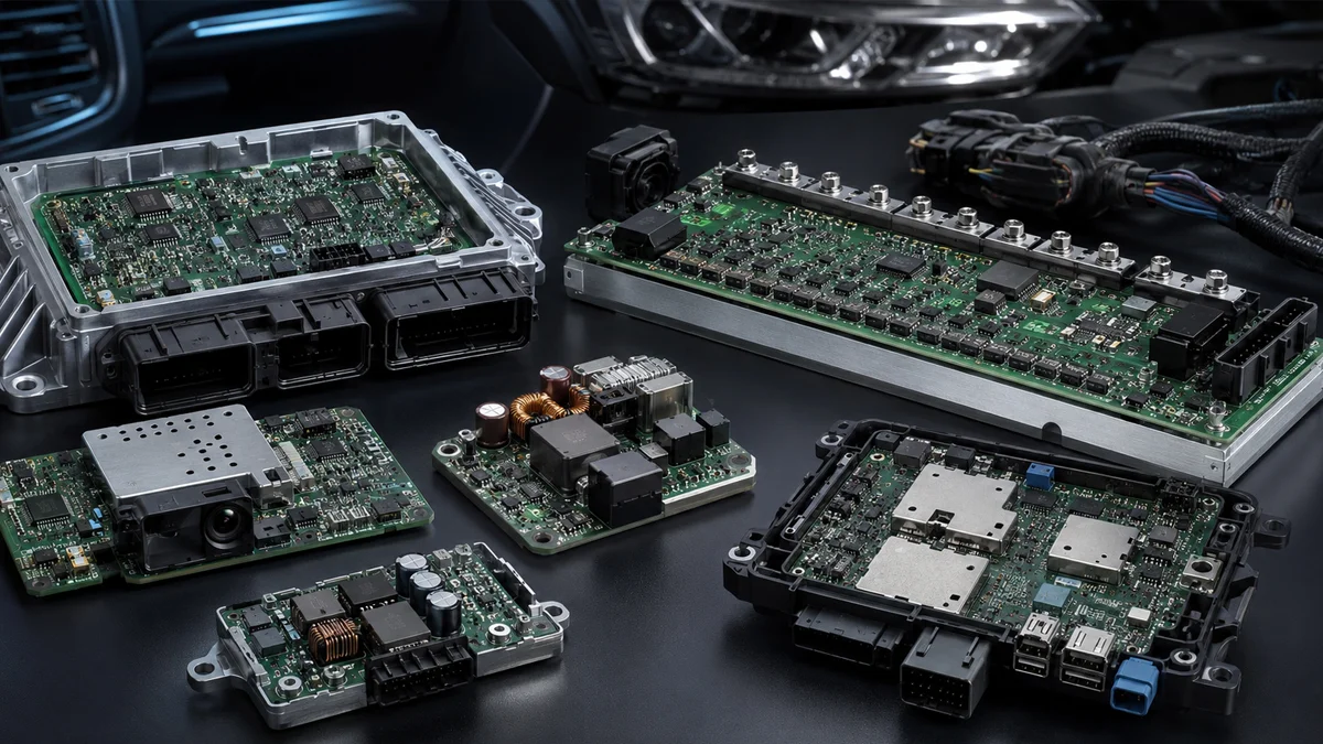
Automotive control, sensor, lighting and power modules often contain hidden or high-current solder connections. X-ray inspection helps identify internal solder defects before assemblies enter further testing or final module production.
Medical Device Manufacturing
Medical Electronics
Medical-electronics manufacturers can use saved X-ray images to support controlled inspection, failure analysis and quality documentation.
Telecommunications SMT 1
Telecommunications
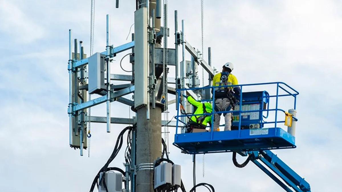
Communication, server and networking boards frequently use BGAs, QFNs and large multilayer assemblies that cannot be fully examined through visual inspection.
Semiconductor Packaging
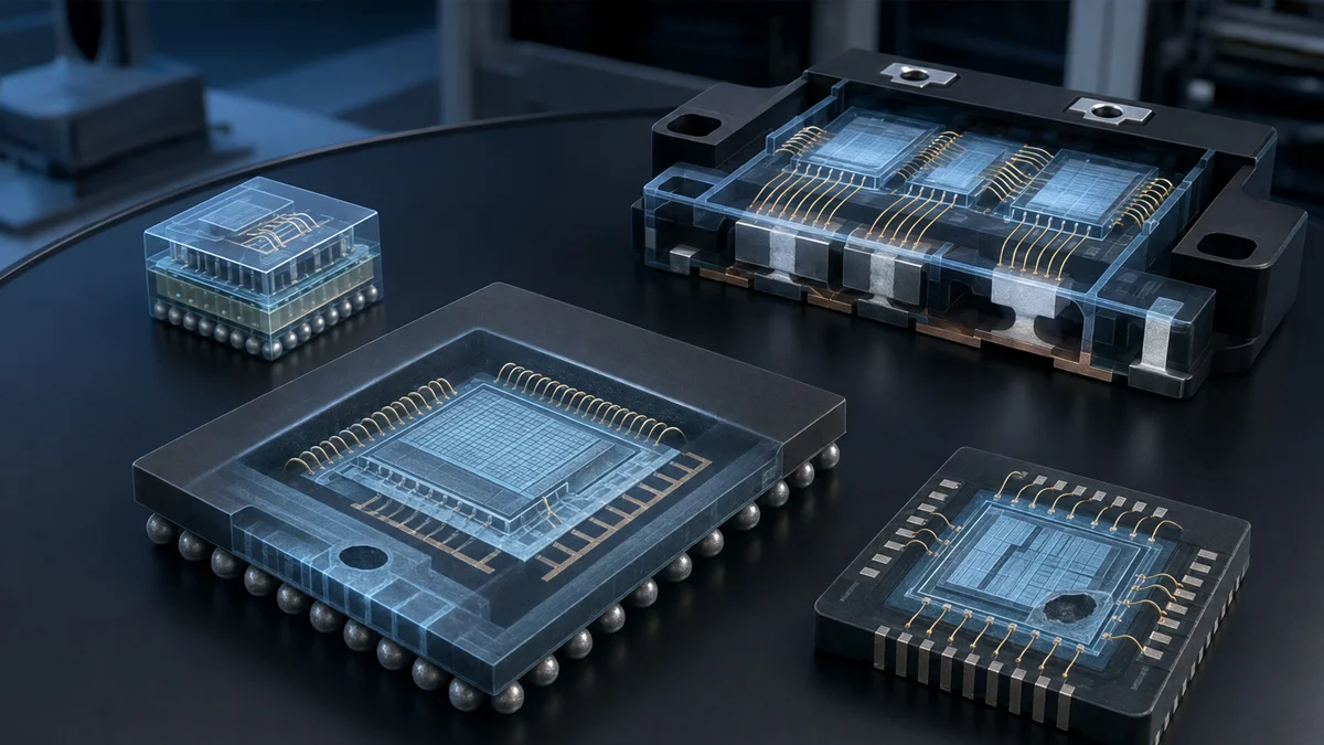
Compatible semiconductor packages and modules can be examined for internal structural abnormalities and connection conditions.
Consumer Electronics PCBA
Consumer Electronics
The system can support first-article inspection, process verification and failure analysis for densely assembled consumer-electronics PCBAs.
EMS & Contract Manufacturing
EMS and Contract Manufacturing
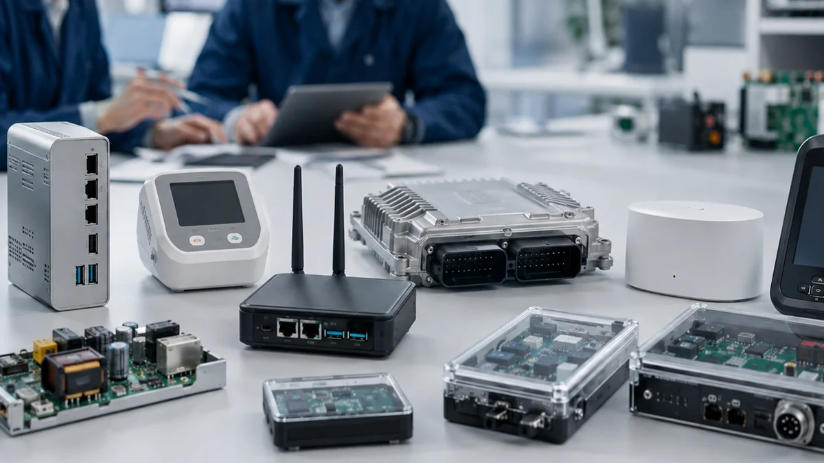
EMS factories process many PCB designs and package types. An offline X-ray system provides a flexible inspection station for first-article verification, hidden-joint quality control and failure analysis across different production lines.

FAQs by PCBA X-Ray Inspection

What can the DEZ-X7600 inspect?

It can inspect PCBA, PCB assemblies, BGA and QFN solder joints, semiconductor packages, connectors and other compatible electronic components.

BGA solder joints are located completely underneath the package and cannot be inspected directly by AOI or visual inspection.

It can help identify voids, solder bridges, missing solder, insufficient solder, irregular joints, package displacement and other internal abnormalities.

No. It is a non-destructive inspection method, so the assembly remains intact after inspection.

Yes. The software includes image calculation and measurement functions for evaluating void areas and other visible features.

The maximum listed inspection range is 510 × 450 mm.

The inspection platform supports samples weighing up to 12 kg.

Yes. The large platform and movable inspection range allow different areas of a large assembly to be positioned for inspection.

Yes. Multi-angle observation helps separate overlapping structures and examine hidden joints from different directions.

The system provides up to 150× geometric magnification.

The DEZ-X7600 is an offline inspection system operated by an inspector. For automatic 100% production-line inspection, an inline AXI system should be evaluated.

No. AOI is better for visible component and surface defects, while X-ray is used for hidden and internal structures. The two systems perform different inspection functions.

Yes. It can inspect the solder joints after BGA removal, rebelling or replacement to verify the rework result.

Yes. Customers can provide PCBAs or electronic components for sample imaging and defect-analysis testing.

Send Your SMT Equipment Requirements

Contact DEZ for PCBA cleaning machine, selective soldering machine, stencil cleaning machines, X-ray inspection, BGA rework, reflow ovens and SMT handling equipment.

Send your workpiece dimensions, production problem and required throughput to receive a free application review, equipment recommendation and project quotation. Free sample testing is available for qualified projects.

An equipment specialist will contact you within one hour during business hours.

Get a Free Recommendation and Request Sample Testing
Email: [email protected]
Phone: +86 138 2338 9052

Drag & Drop Files, Choose Files to Upload, or Capture With Your Camera