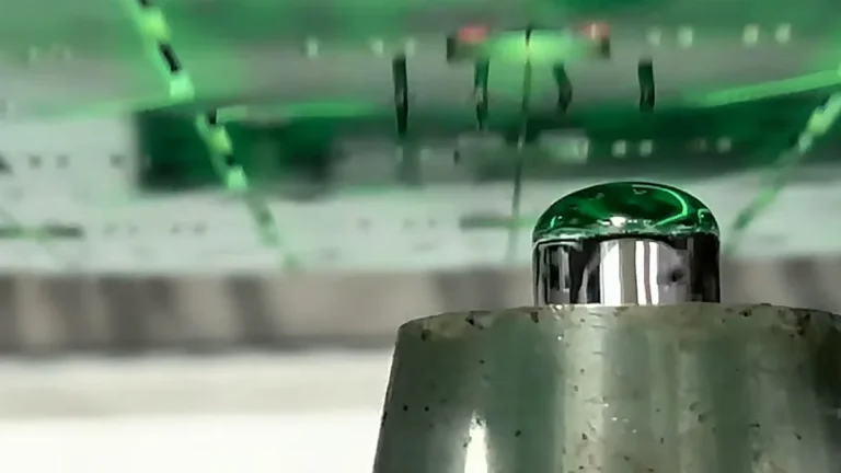
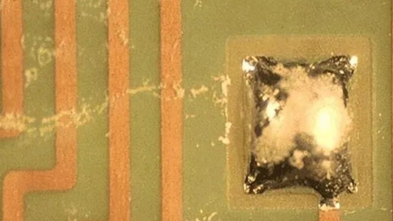
Wave soldering passes most or all of the PCB underside across a solder wave. Selective soldering applies flux, preheats and solders only the specified through-hole joints.
Wave soldering is commonly used when a board contains many accessible THT joints. Selective soldering is better suited to mixed-technology PCBAs where only certain connectors, terminals, relays or other THT components require soldering.
Table of Contents
How Wave Soldering Works
The PCB passes through fluxing, preheating and a full-width solder wave.
All accessible solder joints on the underside contact the molten solder. Areas that must not be soldered may require masking, keep-out space or a soldering pallet.
Wave soldering can process many THT joints in one pass, making it suitable for repeated production of boards designed for the process.
How Selective Soldering Works
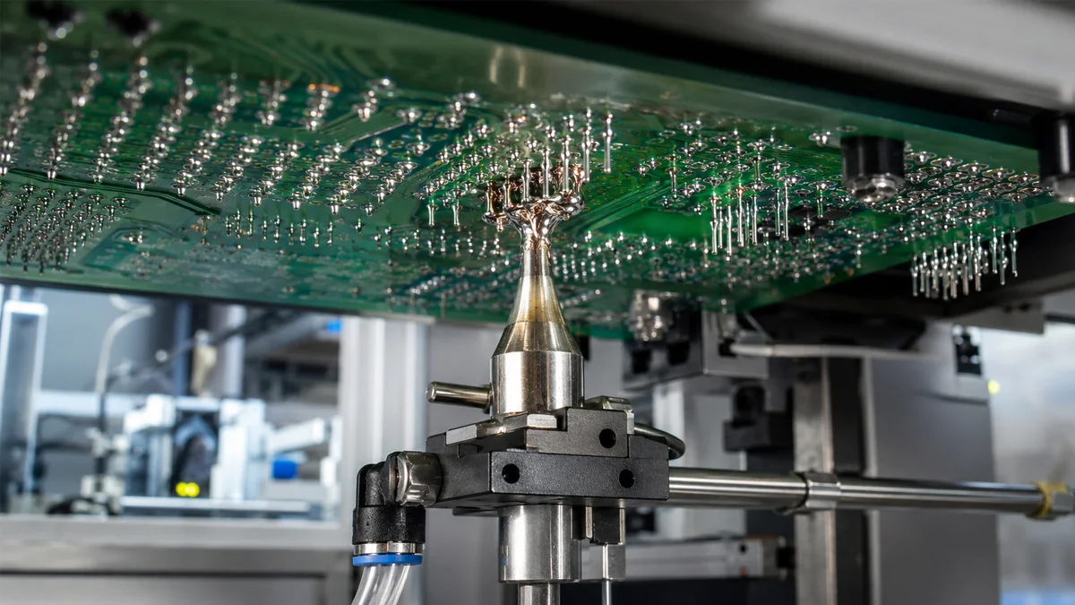
Selective soldering applies flux only to the programmed joint locations. The PCB is preheated before a mini-wave nozzle moves to each soldering position.
The nozzle contacts only the required joints. Nearby SMT components and areas that must avoid molten solder remain outside the solder wave.
Wave soldering requires sufficient clearance across the PCB underside. Bottom-side SMT components, heat-sensitive parts and closely spaced pads can restrict access to the full solder wave.
Selective soldering works with mixed assemblies because the nozzle is programmed to avoid restricted areas. The PCB must still provide enough clearance for the selected nozzle and solder-wave diameter.
Check the bottom-side component height, keep-out areas and distance between THT joints before selecting the process.
Number of THT Joints
Wave soldering is generally more productive when almost the entire board contains accessible through-hole joints.
Selective soldering becomes practical when only a limited number of connectors, terminals, relays or transformers require soldering after SMT reflow.
The selective soldering cycle increases with the number of soldering positions, travel distance and required dwell time.
Heat Exposure
Wave soldering exposes a large section of the PCB underside to molten solder.
Selective soldering limits direct solder contact to the programmed joints. This helps process assemblies containing nearby SMT components or heat-sensitive areas that cannot pass through a full solder wave.
Preheating remains necessary to activate the flux, reduce thermal shock and support hole fill.
Flux Application
Wave soldering normally applies flux across a broader PCB area.
Selective soldering deposits flux at the required THT positions. Flux quantity, spray pattern and location can be programmed according to the assembly.
Too little flux can cause poor wetting and insufficient hole fill. Excess flux can leave more residue or spread towards areas that do not require soldering.
Soldering Nozzles
Wave soldering uses a solder wave wide enough to contact the required underside area.
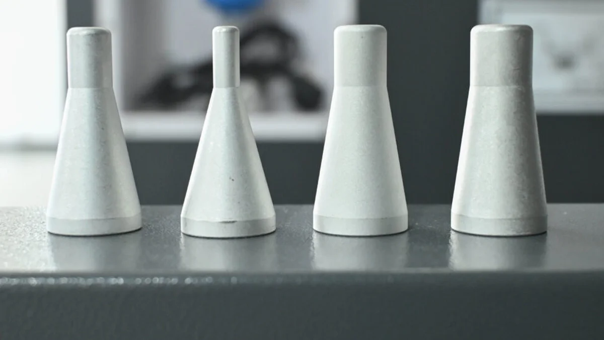
Selective soldering uses mini-wave nozzles selected according to the joint group, component clearance and soldering path.
A larger nozzle may solder multiple nearby pins more quickly. A smaller nozzle provides access around closely spaced components but may increase the cycle time.
Throughput
Wave soldering can be faster when many joints must be soldered across every PCB.
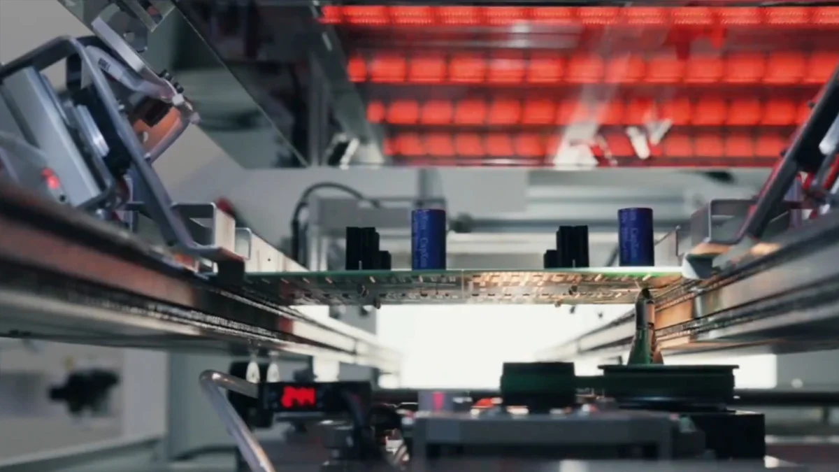
Selective soldering throughput depends on fluxing, preheating, nozzle movement, soldering time and the number of joint locations. Inline systems can separate or overlap process stages to support continuous production.
Compare the required boards per hour using the actual PCB program rather than the machine travel speed alone.
Product Changeovers
Wave soldering changeovers may require new pallets, masking and process settings.
Selective soldering stores fluxing and soldering coordinates as recipes. A product change may still require a different carrier, nozzle, conveyor width or preheating setting.
High-mix production benefits from verified programs and controlled changeover procedures.
Solder-Joint Quality
Neither process automatically guarantees better solder joints.
Bridging, insufficient hole fill, poor wetting and solder icicles can occur with either method. The result depends on pad and hole design, component lead condition, flux, preheating, solder temperature, contact time and withdrawal settings.
Inspect the joints and adjust the process using the actual PCB assembly.
When to Choose Wave Soldering
Choose wave soldering when the PCB contains many accessible THT joints, the underside is designed for full-wave contact and the same product will be manufactured repeatedly.
It is also suitable when the required throughput makes joint-by-joint soldering impractical.
When to Choose Selective Soldering
Choose selective soldering when only specified THT components require soldering, the PCB contains bottom-side SMT components or some areas must avoid molten solder.
It is also suitable for high-mix production, assemblies with localised through-hole connectors and processes that require programmable flux and soldering paths.
Can Both Processes Be Used?
Yes. A manufacturer may use wave soldering for boards with many suitable THT joints and selective soldering for mixed assemblies or remaining components that cannot pass through the wave process.
The selection should be made by PCB design and production method rather than applying one process to every product.
Selecting a Selective Soldering Machine
Provide the PCB or carrier dimensions, board thickness, THT joint coordinates, bottom-side component clearance, solder alloy, flux, nozzle requirements and target cycle.
Use an offline machine for independent batch loading. Use an inline machine when PCBAs must transfer continuously from upstream production equipment.
DEZ selective soldering equipment includes compact, offline and inline configurations for different PCB dimensions and production methods.
Request a Soldering Evaluation
Send your PCB drawing, THT solder-joint positions, component-clearance information and required throughput. DEZ can review the assembly and recommend the relevant selective soldering configuration.