BGA, QFN, LGA and CSP solder joints are located beneath the component package. Once soldering is complete, these connections cannot be fully inspected with a camera or microscope.
X-ray inspection creates an internal image of the package, solder joints, pads and other structures without dismantling the PCB assembly.
Why Visual Inspection Is Not Enough
Visual inspection can confirm component position, polarity and visible solder joints. It cannot show the complete solder structure beneath a bottom-terminated package.
A BGA may appear correctly positioned while containing voids, bridges, insufficient solder or missing connections underneath. These defects may cause immediate functional failure or intermittent problems during operation.
What X-Ray Inspection Can Detect
Voids
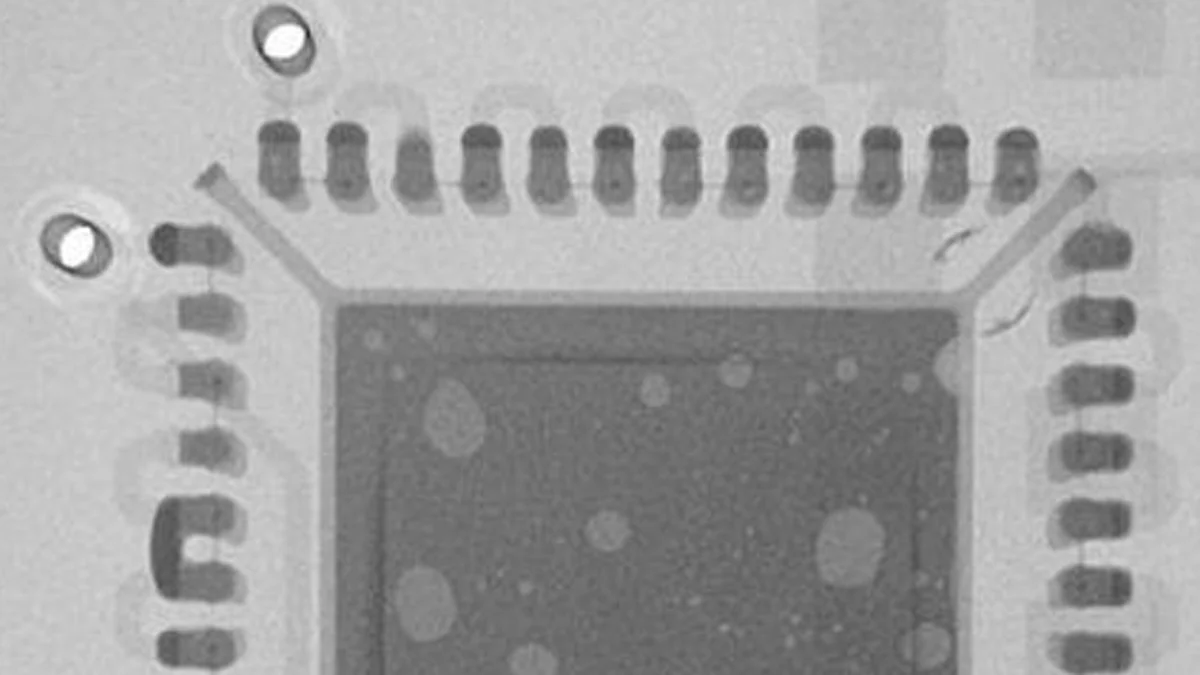
Voids appear as lighter areas inside the darker solder joint image. X-ray allows the operator to examine their size, number and position.
Void acceptance cannot be determined from appearance alone. The permitted level depends on the package, solder joint, customer specification and inspection method.
Solder Bridges
Bridges appear when solder connects two adjacent balls or pads that should remain electrically separate.
X-ray is particularly useful when the bridge is completely hidden beneath the package.
Insufficient Solder
A joint with insufficient solder may appear smaller or less dense than surrounding joints.
The operator should compare the suspect joint with other balls in the same row, package and assembly.
Excess Solder
Excess solder can produce enlarged or irregular joint shapes. It may increase the risk of bridging or indicate inconsistent solder-paste deposition.
Missing Solder Joints
A missing ball, incomplete paste deposit or open connection may appear as an empty or irregular position within the BGA pattern.
Some open-joint conditions are difficult to prove using a single 2D image. Electrical testing or additional inspection may still be required.
Package Misalignment
X-ray can show whether the BGA balls are centred over the PCB pads and whether the package shifted during reflow.
Irregular Ball Shape
Uneven, elongated or distorted solder images may indicate movement, poor wetting, excessive solder or another process abnormality.
How BGA X-Ray Inspection Works
The PCB assembly is positioned inside the shielded inspection cabinet. The X-ray source passes radiation through the sample, while the detector records differences in material thickness and density.
Dense materials such as solder absorb more X-rays and appear darker in the image. Voids, gaps and lower-density areas appear lighter.
The operator adjusts the sample position, magnification, image contrast and X-ray settings to examine the package and individual solder joints.
Inspect the Complete BGA Pattern
Begin with a full view of the BGA to check package position and solder-ball distribution.
Compare rows, columns, corners and centre joints. Look for missing balls, bridges, inconsistent sizes and unusual density.
After identifying a suspect area, increase the magnification and inspect the joint in relation to neighbouring solder balls.
Compare Similar Solder Joints
A single joint should not be evaluated without context.
Compare joints with similar pad size, ball size and thermal conditions. Corner, centre and ground-pad connections may produce different X-ray appearances because their copper areas and heat transfer are different.
Reference images from known-good assemblies can improve inspection consistency.
X-Ray Inspection After Reflow
X-ray inspection can be used during first-article production to confirm that the reflow process creates acceptable hidden solder joints.
If defects are found repeatedly in the same location, review the solder-paste printing, stencil design, component placement, pad condition and reflow temperature profile.
X-ray identifies the internal result. It does not identify the root cause automatically.
X-Ray Inspection After BGA Rework
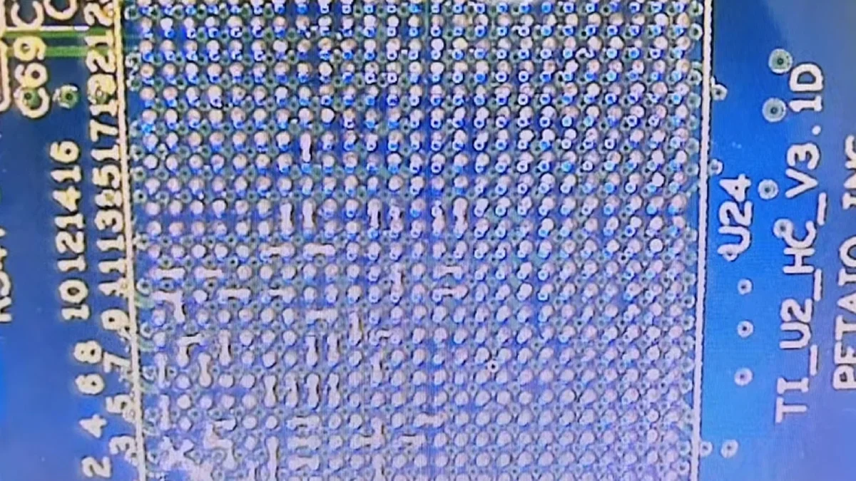
A replaced BGA should be inspected after reflow to check alignment, bridging, voids and solder-ball consistency.
The usual process is:
X-Ray Inspection → Defect Evaluation → BGA Removal → Pad Preparation → Component Alignment → Reflow → Post-Rework X-Ray Inspection
Electrical and functional testing should follow when required by the assembly specification.
X-Ray Inspection Does Not Replace Other Tests
X-ray inspection examines internal structures, but it cannot confirm every aspect of PCB assembly quality.
It does not measure ionic contamination, prove solder-joint mechanical strength or confirm complete electrical functionality. Some defects may also require angled inspection, computed tomography, cross-section analysis or electrical testing.
Use X-ray together with visual inspection, AOI, electrical testing and functional testing according to the product requirements.
When Should BGA Joints Be Inspected?
First Production
Inspect the first assemblies after setting the printing, placement and reflow process.
Reflow Profile Changes
Repeat inspection after changing the solder paste, stencil, component, conveyor speed or temperature profile.
Process Failure Analysis
Use X-ray when functional testing indicates a possible hidden solder-joint problem.
BGA Rework
Inspect before rework to identify the defect and after rework to verify the new solder structure.
Process Monitoring
Periodic inspection can detect changes in printing, placement and reflow before they affect a larger production batch.
Selecting a PCBA X-Ray Inspection System
Start with the PCB and component dimensions, package type and defects that must be inspected.
Also confirm the required image resolution, magnification, field of view, sample positioning, image storage and production volume. Requirements for angled viewing, automated inspection or production-system connection must be specified before selecting the equipment.
The inspection requirement should determine the system configuration—not magnification alone.
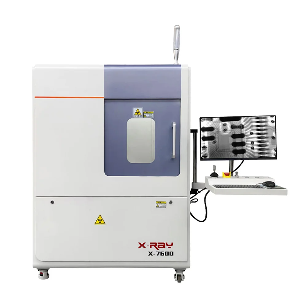
DEZ-X7600 PCBA X-Ray Inspection System
The DEZ-X7600 is used for non-destructive inspection of BGA, QFN, LGA, CSP and other components with hidden solder connections.
It helps operators examine voids, bridges, insufficient solder, missing connections and package misalignment during process development, production inspection and failure analysis.
View DEZ-X7600 X-Ray Inspection System
X-Ray Inspection and BGA Rework
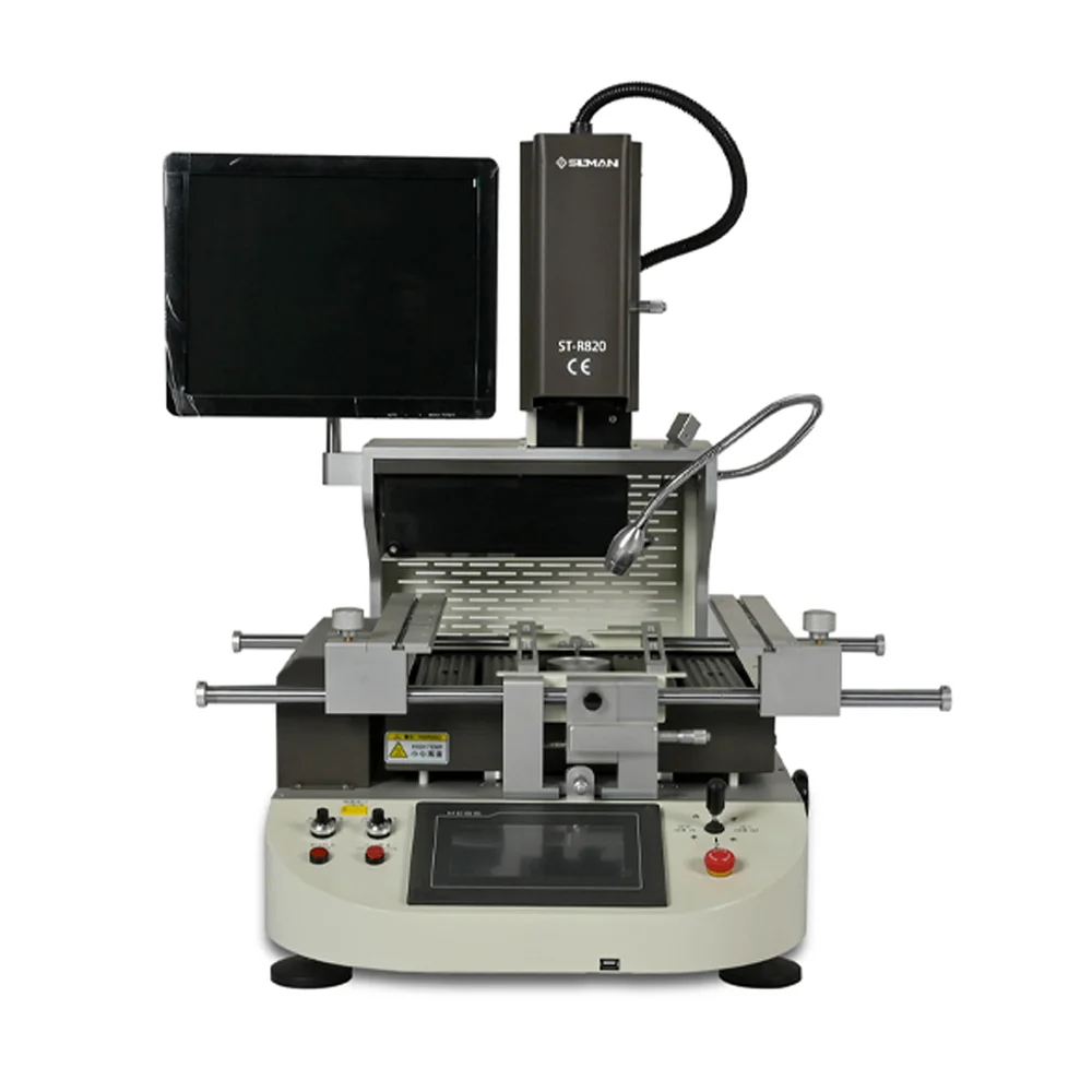
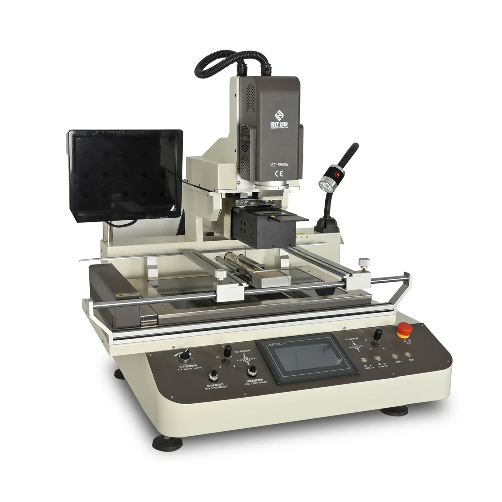
When inspection confirms that a package must be replaced, DEZ provides two BGA rework configurations.
The DEZ-R820 Semi-Automatic BGA Rework Station uses controlled heating and optical alignment for BGA, QFN and CSP replacement.
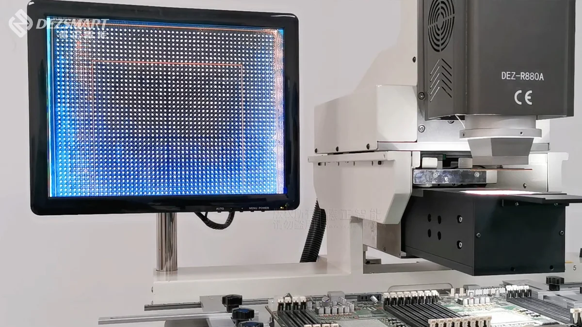
The DEZ-R880A Automatic BGA Rework Station adds servo-controlled movement, optical alignment and programmable heating for automated rework operations.
Request an X-Ray Inspection Test
Send the PCB dimensions, package type, component size and defect to be inspected. Sample PCBAs and existing X-ray images can be used to evaluate the inspection requirement.