White residue, a sticky film and loose solder balls are three different post-soldering conditions. They should not be treated as one general “dirty PCB” problem.
White residue may originate from flux, the cleaning process or the solder mask. A sticky film usually points towards remaining organic material or an incomplete cleaning process. Loose solder balls are metallic particles produced by soldering, printing, handling or material conditions.
None of these observations identifies the root cause by itself. The first question is not simply how to remove the contamination, but when it appeared, where it is located and which process created it.
Observation
What it may indicate
What appearance alone cannot confirm
White powder, haze or spots
Flux residue, incomplete rinsing, cleaner incompatibility, poor solder-mask cure or a material change
Ionic contamination or corrosion risk
Sticky or tacky film
Remaining rosin or resin, incompletely conditioned flux, excessive flux, cleaning-agent mismatch or partial cleaning
Whether the residue is electrically harmful
Loose solder balls
Printing, placement, reflow, wave or selective-soldering instability
Which process parameter created the balls
Table of Contents
PCB White Residue
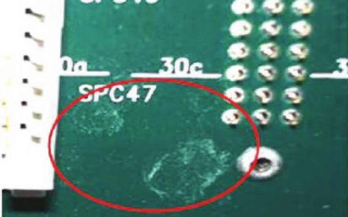
White residue can look like powder, haze, rings or crystalline spots around solder joints and across the solder mask. Its timing and location provide the first useful evidence.
If it appears immediately after soldering and before cleaning, investigate the flux, preheat, thermal profile and PCB material. Insufficient thermal exposure may leave flux activators or carrier materials incompletely conditioned.
If it appears only after cleaning, inspect the cleaning chemistry, bath loading, rinse-water quality, rinse coverage and drying stage. A cleaner that worked with one solder paste may not remove another formulation under the same settings.
If white spots follow a particular PCB batch or appear within the solder-mask surface, incomplete solder-mask cure or material incompatibility may be involved. ZESTRON documents partially cured solder mask, solder-paste changes and rinse-medium conditions as separate possible causes of white spots.
White colour does not prove that the residue is ionic, corrosive or electrically conductive. Determine the risk through analysis and testing rather than appearance.
How to Cleaning PCB White Residue
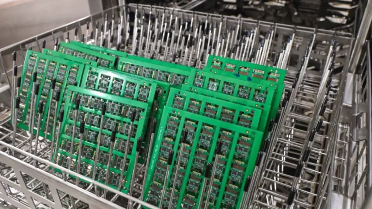
For full-board cleaning, the process normally requires compatible chemistry, controlled washing, DI-water rinsing and drying.
The DEZ-C743 offline PCBA cleaning machine is suitable for high-mix batch cleaning. It completes chemical spray washing, DI-water rinsing and hot-air drying inside one chamber.
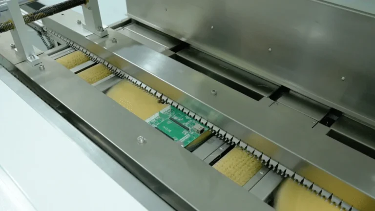
For continuous production, the DEZ-C1360 inline PCBA cleaning machine conveys assemblies through chemical washing, DI-water rinsing and two hot-air drying zones.
If the residue is confined to an accessible solder joint, lead, connector or rework area and a waterless process is required, the DEZ-C7310 PCBA dry ice cleaning machine can be evaluated through sample testing. It should not be used as proof that an ionic-cleanliness requirement has been met.
Sticky Film from PCB
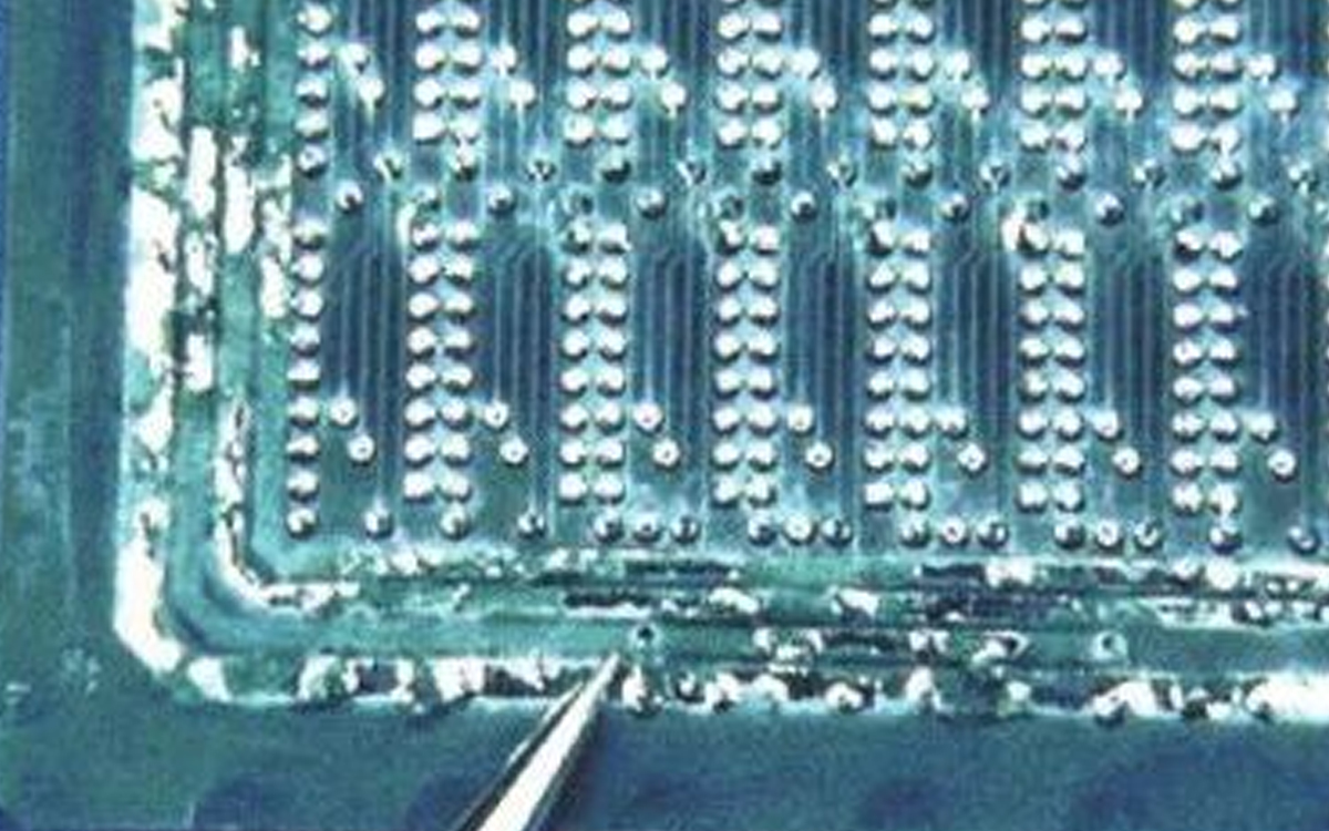
A sticky surface usually indicates that organic material remains on the assembly. Possible sources include rosin or synthetic-resin flux, tacky rework flux, adhesive, handling contamination or partially removed residue.
“No-clean” does not mean residue-free. A no-clean flux may leave a qualified residue when it receives the intended thermal exposure and remains undisturbed. Its acceptability depends on the material specification, assembly design, electrical environment and downstream processes.
Unexpected tackiness may indicate:
Excessive or uneven flux application
Insufficient preheat or thermal exposure
Flux outside its specified process window
Cleaning chemistry that does not dissolve the residue
Short wash time or weak mechanical action
Partial wiping that redistributes residue across a larger area
Contaminated brushes, filters or cleaning liquid
Flux residue can remain tacky or become hard depending on its chemistry and thermal history.
Cleaning Sticky Flux from an Accessible Solder Side
When the film is concentrated on one accessible solder-side surface, full-board aqueous cleaning may be unnecessary.
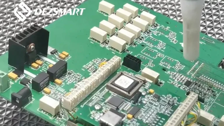
The DEZ-C758 single-sided PCBA cleaning machine applies a compatible cleaning agent before multidirectional wet brushing, dry brushing and fan drying. It supports PCBA widths of 50–300 mm and component heights up to 135 mm.
The DEZ-C760 automatic PCBA brush cleaning machine uses one 360 mm rotary brush and two roller brushes after applying alcohol-based PCBA cleaning fluid. It processes PCBAs up to 300 × 300 mm and requires at least 1.5 mm of available board edge for gripping.
Brush cleaning is suitable only when the residue is physically accessible. If contamination extends beneath low-standoff components or must be removed from the complete assembly, use an aqueous wash-and-rinse process instead.
Avoid uncontrolled partial cleaning. Research on rework contamination indicates that unsuitable IPA cleaning and contaminated swabs or brushes can redistribute residue or introduce cross-contamination.
PCB Loose Solder Balls
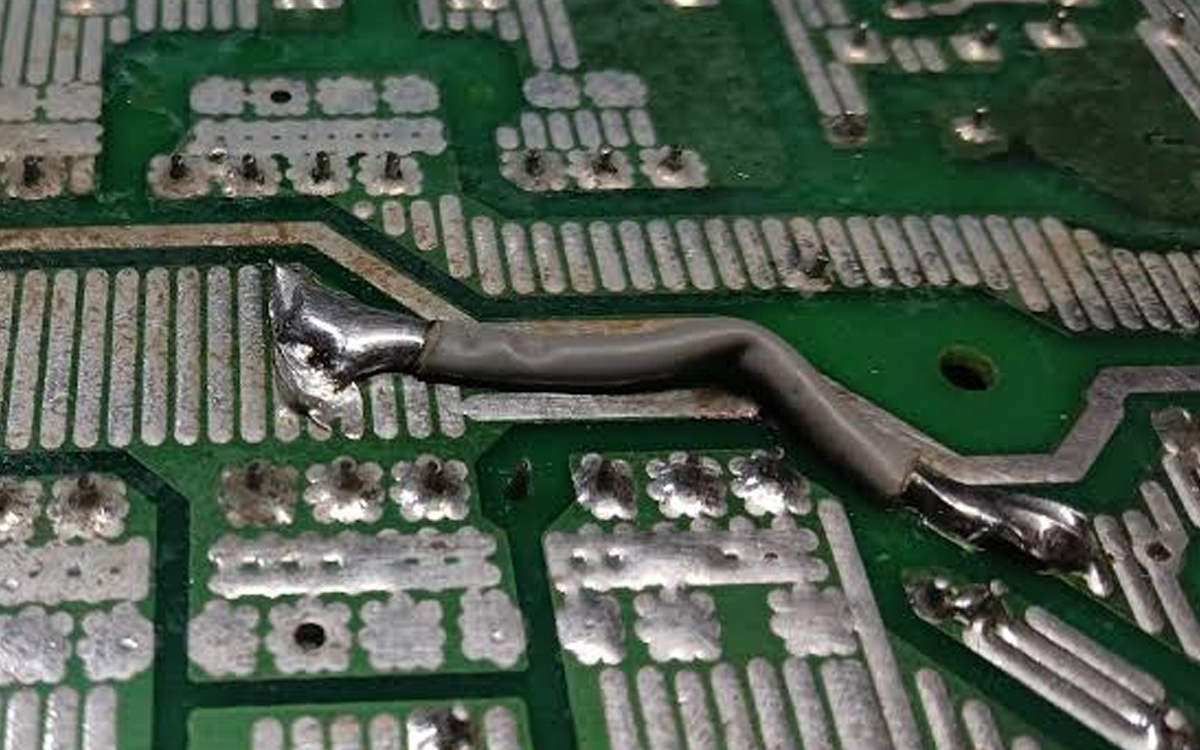
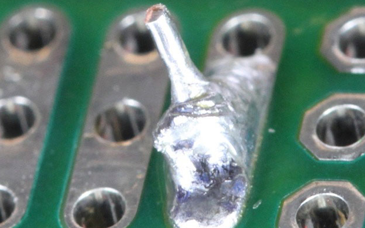
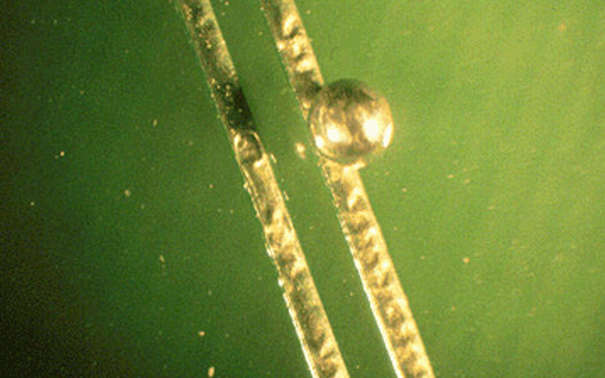
Loose solder balls are metallic particles located around joints, beneath components or across the assembly surface. Unlike a cosmetic flux mark, a mobile solder ball can move between conductive features and create a short-circuit risk.
After Reflow Soldering
Solder balls around chip components or beside paste deposits may relate to:
Excess or misplaced solder paste
Paste slumping before reflow
Contamination on the stencil underside
Excessive placement pressure
Inappropriate pad, stencil or aperture design
Rapid solvent outgassing
Solder paste transferred by dirty tools or manual handling
AIM Solder documented a case where persistent solder balling was ultimately traced to contaminated tweezers transferring solder paste—not the reflow profile. This illustrates why the defect must be traced through the complete process rather than assigned to oven temperature alone.
After Wave or Selective Soldering
Solder balls or spatter on the solder side may indicate:
Insufficient preheat
Moisture in the PCB or process materials
Uneven or excessive flux application
Trapped flux or gas around PTHs
Excessive solder turbulence
Incorrect board contact with the solder wave or nozzle
Solder-mask or laminate conditions that promote solder adhesion
Cleaning removes loose solder balls already present on the assembly, but it does not correct the process that formed them. Preheat, flux deposition, board condition, nozzle or wave settings and material storage must be checked separately.
Removing Accessible Loose Solder Balls
The DEZ-C758 and DEZ-C760 use controlled brush contact to dislodge accessible loose solder balls from the solder side and direct removed waste into the collection area.
Choose:
DEZ-C758 for continuous single-sided processing with cleaning-agent application, wet brushing, dry brushing and fan drying.
DEZ-C760 when the board fits within 300 × 300 mm and multidirectional rotary and roller-brush contact is required.
Neither machine can guarantee removal from inaccessible spaces beneath components. Inspect representative samples after cleaning and confirm that brush contact is compatible with leads, joints and bottom-side components.
Select the Cleaning Process by What Must Be Removed
Production condition
Suitable DEZ process
Visible flux marks or loose solder balls on one accessible solder side
DEZ-C758 or DEZ-C760
White or sticky residue across a high-mix batch of complete PCBAs
DEZ-C743
Continuous full-board washing, DI-water rinsing and drying
DEZ-C1360
Local, accessible flux or rework residue requiring waterless cleaning
Soldering process: reflow, wave, selective or manual
DEZ can use this information to separate the visible symptom from its likely process source and test the correct brush, aqueous or dry-ice cleaning method before equipment selection.