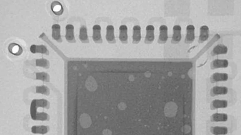
A BGA X-ray inspection machine allows engineers to inspect solder joints hidden underneath BGA, CSP, QFN and LGA packages.
Unlike leads around a QFP or visible joints on a through-hole component, BGA solder balls are located between the component body and the PCB. AOI and visual inspection can verify component position and surrounding conditions, but they cannot directly inspect the complete hidden solder pattern.
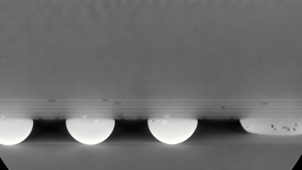
X-ray imaging solves this visibility problem by showing differences in the projected density and shape of the solder joints. It can reveal bridges, missing balls, voids, abnormal solder volume and package misalignment before an assembly moves to the next production stage.
However, an X-ray image is not a complete electrical or reliability test. Some opens, head-in-pillow defects and microcracks may require angled imaging, CT, electrical testing or destructive analysis for confirmation.
Table of Contents
Why Hidden BGA Joints Need X-Ray Inspection
A BGA package can appear correctly positioned while still containing defects underneath.
A solder bridge may connect two adjacent balls. One position may contain insufficient solder or no ball at all. Voids can occupy part of a joint, while uneven reflow or package movement can shift the solder pattern away from the PCB pads.
These defects are especially costly when they are discovered after final assembly. The product may already have entered functional testing, system integration or customer use, making diagnosis and rework much more difficult.
For this reason, BGA X-ray inspection and rework should be treated as a controlled process rather than simply taking an image and making a quick visual judgment.
How BGA X-Ray Imaging Works
An X-ray inspection system contains three essential parts: an X-ray source, the PCBA being inspected and a digital detector.
The source emits X-rays through the assembly. Materials with different thicknesses and densities attenuate the radiation differently. The detector converts these variations into a grayscale image that shows the projected structure of solder, copper, component materials and PCB layers.
The image can then be used to compare solder-ball shape, size, spacing and internal void distribution.
The required tube voltage depends mainly on the penetration needed for the sample. Tube current or output affects image brightness and acquisition speed, while focal-spot size influences image sharpness—particularly at high geometric magnification. These parameters must be considered together rather than evaluated as isolated specification numbers.
Magnification Is Not the Same as Resolution
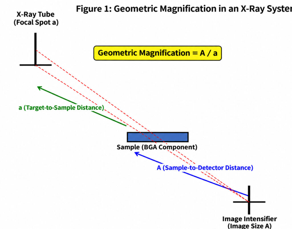
Geometric magnification is determined by the relationship between the source, sample and detector:
Moving the PCBA closer to the X-ray source increases magnification. But a larger displayed image does not automatically contain more useful detail.
Effective inspection quality also depends on:
X-ray focal-spot size
Detector pixel size and imaging area
Image contrast and noise
Mechanical stability
Sample thickness and material density
Viewing angle
Excessive magnification can reduce the field of view and make it harder to inspect the complete BGA pattern efficiently. If source blur, detector resolution or vibration becomes the limiting factor, increasing geometric magnification only enlarges the blur.
The practical goal is therefore not the highest available magnification. It is the clearest repeatable image of the smallest defect the factory needs to identify.
Why a Top-Down Image May Not Be Enough
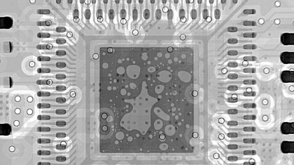
A top-down view is useful for checking the complete solder-ball grid. Missing balls, major bridges, abnormal ball size, misalignment and void distribution can often be recognized quickly.
The limitation is that a 2D X-ray image compresses every structure along the beam path into one projection. Copper layers, nearby components and solder features may overlap.
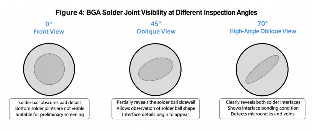
An angled view changes this projection. It can separate overlapping structures and provide more information about solder geometry, wetting position and suspicious interfaces.
This does not mean every crack or open joint becomes visible simply by changing the angle. Detectability still depends on the size, orientation and density contrast of the defect. Multiple viewing angles improve the evidence available to the engineer, but electrical testing or cross-section analysis may still be required.
What BGA Defects Can X-Ray Reveal?
Condition
Typical X-ray evidence
Important limitation
Solder bridge
A continuous solder path appears between adjacent positions
Confirm that the apparent connection is not caused by overlapping copper or another board layer
Missing ball or insufficient solder
One position has missing or abnormally small projected solder area
Compare with surrounding joints and known-good samples
Voids
Lower-density areas appear inside the projected solder joint
Use a consistent measurement method and customer-defined acceptance criteria
Misalignment
The solder-ball pattern is offset from the expected pad or package position
Small offsets require calibrated measurement rather than visual estimation
Open, head-in-pillow or crack
A separation or abnormal joint profile may be visible from a suitable angle
Some defects may not be conclusive in conventional 2D imaging and need CT, electrical testing or cross-section analysis
X-ray can also support process monitoring by measuring solder-ball area, diameter, roundness, spacing and void percentage. These measurements are most useful when the same imaging conditions and evaluation rules are applied across production batches.
Acceptance criteria should come from the customer’s product requirements and applicable manufacturing standards. A void visible in the image is not automatically a reject unless it exceeds the defined limit or affects the critical joint area.
2D, Multi-Angle or CT Inspection?
Conventional 2D X-ray is suitable for routine offline inspection of bridges, missing solder, void distribution and alignment. It is relatively fast and makes it possible to inspect several components on the same assembly.
Multi-angle imaging is useful when PCB layers or surrounding structures overlap the area being evaluated. It gives the engineer additional projections without requiring a complete 3D reconstruction.
CT reconstructs sectional images so that structures at different depths can be separated. It is valuable for complicated overlapping assemblies, detailed failure analysis and cases where a 2D projection cannot isolate the suspected defect.
CT is not automatically the best choice for every production line. It generally requires longer acquisition and reconstruction time. For routine BGA quality control, clear 2D imaging combined with practical angled views may provide a better balance between defect visibility and inspection speed.
What to Check Before Selecting a Machine
The source specification should be evaluated as a combination of penetration, focal-spot size and operating stability. A high tube-power figure alone does not prove that the system will resolve small BGA defects.
Detector performance is equally important. Pixel size affects the sampling of fine details, while the active imaging area determines how much of the PCB can be viewed at one time. Frame rate influences positioning and live inspection efficiency.
The mechanical platform must accommodate the actual PCB dimensions and weight. It should also provide sufficient travel to inspect components near the board edges without complicated repositioning.
Finally, inspect the software workflow. Operators need practical functions for image adjustment, void measurement, dimensional comparison, image storage and report generation—not merely a high maximum magnification number.
It uses a 130 kV closed microfocus X-ray source with a listed 5 μm focal spot and up to 150× geometric magnification. The flat-panel detector provides a 130 × 130 mm imaging area, 1536 × 1536 resolution, 85 μm pixel size and a 20 fps frame rate.
The system supports multi-angle inspection and accommodates samples up to 510 × 450 mm within its inspection area, with a maximum listed sample weight of 12 kg. These specifications should still be verified with the customer’s actual PCB, package size and target defects before machine selection.