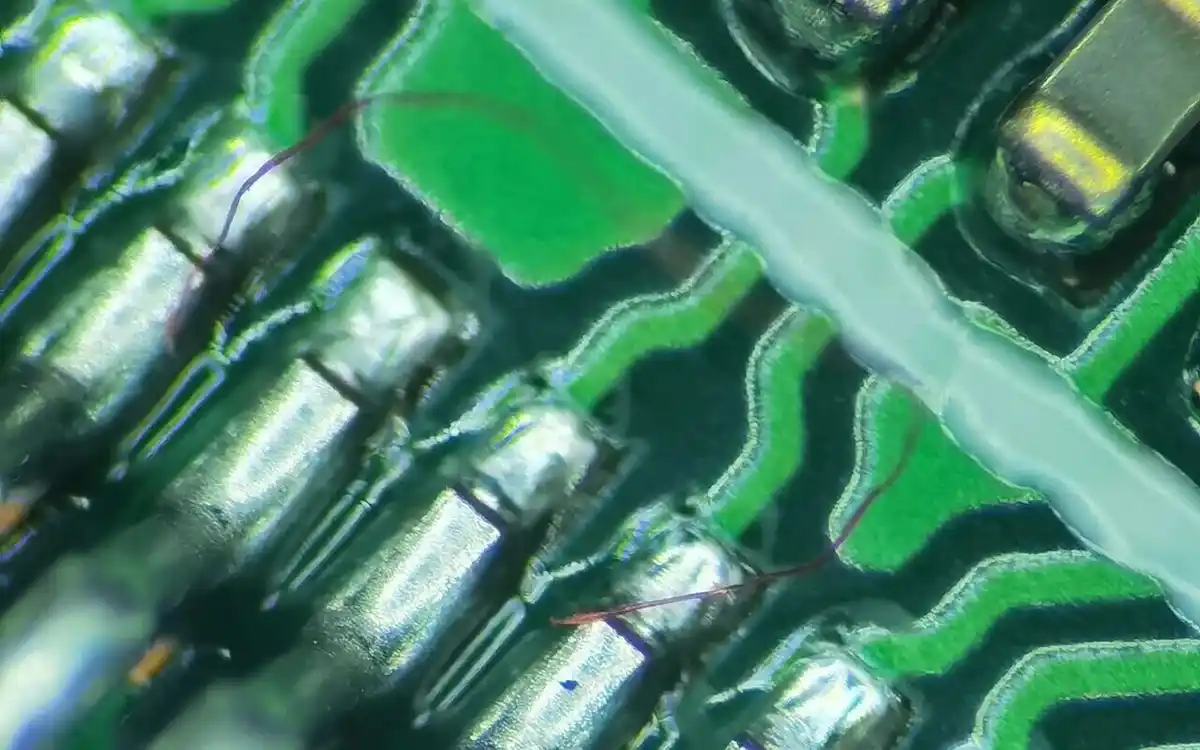
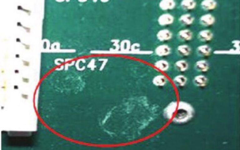
An unclean PCB surface can cause solder paste printing defects when dust, fibres, routing debris or other loose particles interfere with stencil-to-board gasketing, obstruct part of a solder pad or transfer onto the stencil underside.
The resulting print may show insufficient paste, irregular deposit edges, smearing, excessive paste or wet bridging between adjacent pads. However, these defect signatures are not exclusive to PCB contamination. Stencil condition, board support, alignment, aperture design, solder paste rheology, squeegee pressure and separation settings can produce similar results.
The correct approach is therefore to connect the observed defect to its physical mechanism, verify it before reflow and then apply the appropriate corrective action.
Table of Contents
How PCB Surface Contamination Affects Solder Paste Printing
During stencil printing, the PCB is supported beneath the stencil and raised into contact with it. The stencil should gasket against the board around each aperture so that the solder paste is deposited only onto the intended pad area.
Loose contamination changes this interface.
Contamination mechanism
Effect at the print interface
Possible print defect
Appropriate response
A particle is trapped between the stencil and PCB
The stencil is lifted locally and cannot gasket against the solder mask or pad
Smeared deposit, excessive paste, poor edge definition or a wet bridge
Remove loose particles before printing and confirm board flatness and support
A particle covers part of a solder pad
Part of the intended deposit cannot contact the pad correctly
Reduced paste area, irregular deposit or locally insufficient paste
Inspect and clean the incoming PCB before another print
A particle reaches a stencil aperture
Paste filling or aperture release becomes inconsistent
Incomplete deposit, missing paste or deposit-volume variation
Inspect the aperture and stencil underside; clean the PCB and stencil as required
Contamination transfers from the PCB to the stencil underside
The contamination affects subsequent boards, even if the original dirty PCB has left the printer
Repeated smearing, bridging or deposits outside the pad area
Control incoming PCB cleanliness and under-stencil cleaning
Static attracts new particles after handling or loading
A cleaned surface becomes recontaminated before printing
Intermittent defects that vary between boards
Reduce static before particle removal and minimise uncontrolled handling
Contamination or residue on the stencil underside can interfere with gasketing and lead to solder paste in unintended areas or insufficient paste where it is required. It also identifies board coplanarity, solder-mask thickness, alignment and stencil condition as separate variables that can produce similar printing problems.
Poor Gasketing, Smearing and Wet Bridging
Poor gasketing means that the stencil does not make effective contact with the PCB around the aperture being printed.
When a particle creates a local gap, solder paste can spread beneath the stencil instead of remaining within the aperture boundary. The deposit may have an enlarged base, a smeared edge or a thin paste trail extending towards an adjacent pad. If paste connects two deposits before reflow, this is a wet bridge.
After reflow, the same condition may become a solder bridge or produce solder balls, but a post-reflow bridge alone does not prove that the original cause was PCB contamination.
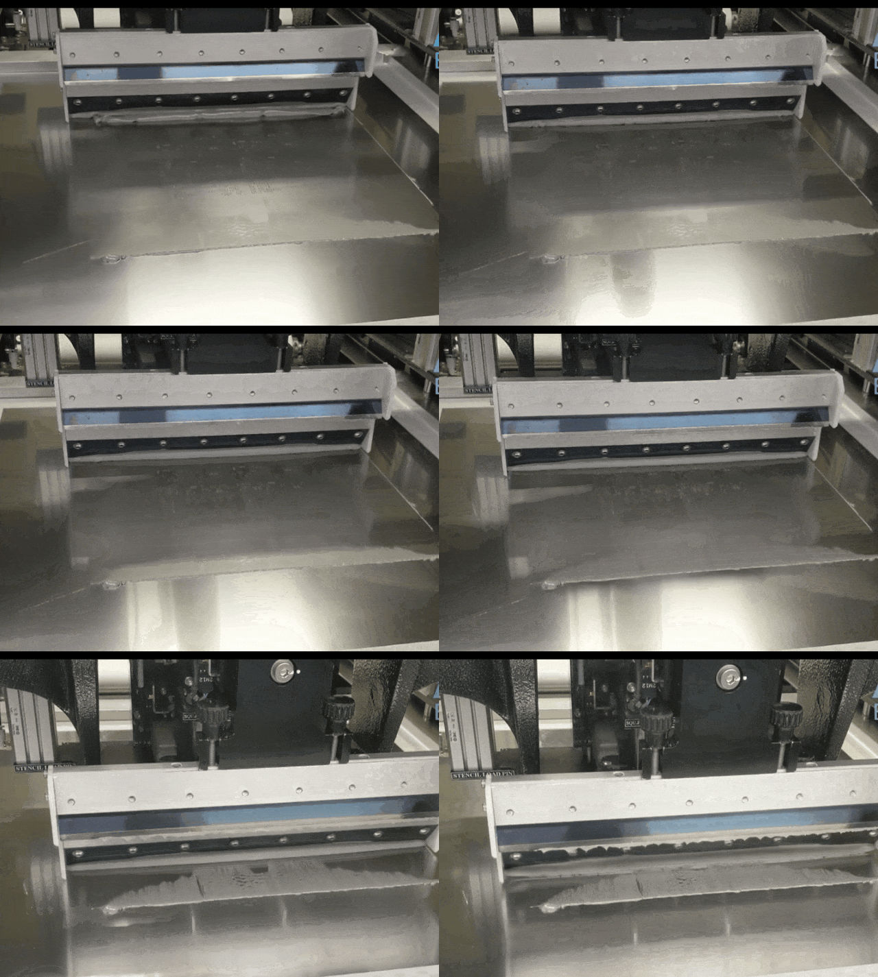
Under-stencil paste produces a similar mechanism. PCEA reports that paste left on the contact side of the stencil prevents effective gasketing and is frequently associated with excessive deposits, solder bridges and solder balls.
This creates an important diagnostic distinction:
A particle arriving on an incoming PCB can initiate the problem.
Paste or contamination retained on the stencil underside can then carry the problem into subsequent print cycles.
Increasing the stencil-wipe frequency may control the secondary contamination but does not remove the original particle source.
PCB cleaning and under-stencil cleaning therefore control different parts of the same print interface.
Insufficient and Incomplete Solder Paste Deposits
A contaminated PCB does not always produce excessive paste. A particle positioned over a pad can reduce the available contact area or disturb paste release as the PCB separates from the stencil.
The SPI result may show:
Reduced deposit area
Low paste volume
Irregular deposit height
A partially missing deposit
Unstable transfer efficiency between consecutive boards
Transfer efficiency is the percentage of the aperture volume transferred onto the PCB. Low or unstable transfer efficiency may also result from an unsuitable area ratio, blocked apertures, worn stencil walls, incorrect solder paste condition or separation behaviour. It should not automatically be attributed to PCB contamination.
Solder paste quantity matters because excessive paste can contribute to shorts, while insufficient paste can reduce the electrical or mechanical integrity of the solder joint.
Is the PCB Surface Really the Root Cause?
The visual appearance of the defect is not enough. Use the defect pattern to decide what to inspect next.
Observed pattern
First checks
Diagnostic interpretation
Defect appears randomly and changes position between boards
Incoming PCB surface, packaging fibres, loader, conveyor and production environment
Loose contamination is a credible cause
Every PCB shows the same defect at the same pad
Stencil aperture, pad design, board support, alignment and local board flatness
A repeatable tooling or process condition is more likely
Smearing or bridging becomes worse over consecutive prints
Stencil underside, wipe interval and contamination transferred from previous boards
Progressive under-stencil contamination is likely
Defect appears immediately after an under-stencil wipe
Stencil dryness, wipe media, solvent compatibility and vacuum cycle
The cleaning cycle itself may be affecting the next print
SPI results are acceptable but bridging, dewetting or solder balls appear after reflow
Placement, paste slump, solderability, oxidation and reflow profile
Do not classify it as a PCB-surface print defect without further evidence
Cleaned and uncleaned boards produce the same SPI distribution
Stencil, paste, printer, support and PCB dimensional conditions
Surface-particle removal is unlikely to be the main corrective action
These patterns are diagnostic clues, not acceptance criteria. The conclusion should come from controlled comparison rather than visual assumption.
AIM’s printing guidance also identifies substrate flatness, board support, separation behaviour, print speed and squeegee pressure as variables that affect paste release and print definition.
Verify the Defect Before Reflow
The most direct way to separate a printing problem from a reflow problem is to inspect the solder paste deposit immediately after printing.
A 2D inspection can evaluate paste coverage, offset and bridging between pads. A 3D SPI system can additionally measure deposit height and volume. IPC technical work identifies area, height, volume and bridge detection as important measurements for evaluating the solder paste printing process.
A practical verification trial should use PCB samples from the same incoming lot:
Divide the samples into cleaned and uncleaned groups.
Keep the stencil, solder paste, printer programme, board support, squeegee and separation settings unchanged.
Inspect both groups with the same SPI programme.
Compare deposit area, height, volume, offset and bridge alarms.
Record whether defects remain at fixed locations or move between boards.
Inspect the stencil underside during the trial for transferred particles or paste smearing.
The trial should use enough boards to reveal repeatability. One visually acceptable print does not demonstrate stable process control.
Which Surface Contaminants Can Be Removed Before Printing?
Dry PCB surface cleaning is suitable for loose contamination such as:
Dust
Fibres and hair
Packaging debris
Routing or depanelisation particles
Loose solder-mask or substrate particles
Static-attracted foreign object debris
These contaminants can usually be loosened, extracted or collected without introducing a liquid washing process before printing.
Oil films, fingerprints, adhesive residue, oxidation and ionic contamination require separate evaluation. A dry particle-cleaning machine should not be presented as a universal method for restoring solderability or chemical cleanliness.
Visible cleanliness also does not prove ionic cleanliness. Ionic contamination requires a specified test method and acceptance criterion.
PCB Cleaning Before Solder Paste Printing
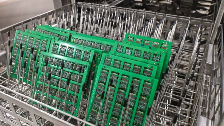
When loose surface particles are confirmed as a print-process variable, install the cleaning stage immediately before the solder paste printer. This reduces the opportunity for the PCB to be recontaminated after cleaning.
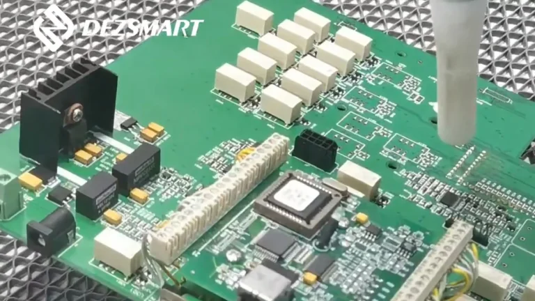
The cleaning process should do more than relocate particles with uncontrolled compressed air. It should reduce static, loosen contamination and capture the released material so that it is not deposited elsewhere on the board or production line.
Three cleaning brushes loosen dust, fibres and loose particles. Ionised air reduces static that can retain contamination, two vacuum sections extract released particles, and front and rear tacky rollers collect remaining debris.
Yes, if a particle prevents the stencil from gasketing against the PCB, solder paste may spread beneath the stencil and towards an adjacent pad. Bridging can also result from stencil contamination, misalignment, excessive paste, poor support or unsuitable printing parameters, so the root cause must be verified.
Can PCB contamination cause insufficient solder paste?
Yes. A particle can occupy part of a pad, interfere with stencil contact or contribute to contamination around an aperture. The result may be reduced deposit area or volume. Repeated low volume at the same location, however, is more likely to indicate an aperture, stencil-design or support problem.
Should every PCB be cleaned before solder paste printing?
Not automatically. The decision should be based on incoming-board cleanliness, packaging and handling conditions, particle sources, product geometry and measured print performance. Inline cleaning is appropriate when loose contamination is a recurring or controlled process risk.
Is compressed-air blowing sufficient?
Airflow may move loose contamination without capturing it and may redistribute particles onto another part of the PCB or production equipment. A controlled cleaning process should combine particle release with extraction or collection.
Does the DEZ-C753S remove flux residue or ionic contamination?
No. The DEZ-C753S removes dry loose contamination from bare PCBs before printing. Flux residue on an assembled PCBA and defined ionic-cleanliness requirements require a different cleaning and verification process.
Control the Cause, Not Only the Defect
An unclean PCB surface can disturb solder paste printing, but the defect should be traced through the print interface rather than inferred from its appearance after reflow.
Inspect the incoming PCB, stencil underside and paste deposit together. Use SPI and controlled comparison to determine whether the defect follows the PCB, remains at a fixed aperture or develops over consecutive print cycles. Once loose surface contamination is confirmed, an inline cleaning process can remove that variable before the PCB reaches the printer.
Send DEZ your PCB dimensions, thickness, contamination samples, conveyor direction and current line configuration to evaluate the DEZ-C753S for your SMT printing process.